High-Throughput Experimentation Effects on National Semiconductor Policies
SEP 25, 20259 MIN READ
Generate Your Research Report Instantly with AI Agent
Patsnap Eureka helps you evaluate technical feasibility & market potential.
HTE Background and Objectives
High-Throughput Experimentation (HTE) represents a paradigm shift in semiconductor research and development, emerging from the convergence of automation, data science, and materials engineering. This approach enables researchers to conduct thousands of experiments simultaneously, dramatically accelerating the discovery and optimization of new semiconductor materials and processes. The evolution of HTE in semiconductors can be traced back to the early 2000s, when combinatorial chemistry methods were first adapted for materials science applications.
The technological trajectory of HTE has been characterized by increasing sophistication in robotics, sensing technologies, and computational methods. Recent advances in artificial intelligence and machine learning have further enhanced the capabilities of HTE platforms, enabling more intelligent experimental design and data interpretation. This evolution has transformed semiconductor research from a largely intuitive, sequential process to a data-driven, parallel approach capable of exploring vast design spaces efficiently.
The primary objective of HTE in the semiconductor context is to compress the traditionally lengthy timeline of materials discovery and process optimization from years to months or even weeks. This acceleration is critical for maintaining the pace of Moore's Law and addressing the increasing complexity of modern semiconductor devices. Additionally, HTE aims to reduce the substantial costs associated with traditional trial-and-error approaches in semiconductor development.
In the national policy context, HTE represents a strategic technology with significant implications for semiconductor sovereignty and competitiveness. Countries leading in HTE capabilities gain advantages in developing next-generation semiconductor technologies, potentially disrupting established industry hierarchies. This has prompted governments worldwide to incorporate HTE into their semiconductor strategies, recognizing its potential as a force multiplier for domestic R&D efforts.
The technical goals for HTE development include expanding the parameter space that can be explored simultaneously, improving the precision and reliability of high-throughput measurements, and developing more sophisticated data analysis techniques to extract meaningful insights from the vast amounts of generated data. There is also a growing focus on integrating HTE with computational methods, creating a feedback loop between simulation and experimentation that further accelerates innovation.
Looking forward, the trajectory of HTE in semiconductors points toward increasingly autonomous experimental systems capable of self-optimization and discovery without human intervention. This represents the ultimate goal of creating truly intelligent research platforms that can navigate the immense complexity of semiconductor materials and processes with minimal human guidance, potentially revolutionizing how semiconductor innovation occurs.
Semiconductor Market Analysis
The global semiconductor market has experienced significant growth over the past decade, reaching approximately $556 billion in 2021 and projected to exceed $1 trillion by 2030. This growth is primarily driven by increasing demand for electronic devices, automotive applications, and the expansion of artificial intelligence and Internet of Things technologies. The market has traditionally been dominated by a few key regions, with East Asia accounting for over 70% of global semiconductor manufacturing capacity.
High-Throughput Experimentation (HTE) is emerging as a transformative approach in semiconductor research and development, enabling rapid testing of multiple materials and process parameters simultaneously. This methodology has begun to influence national semiconductor policies as countries recognize its potential to accelerate innovation and reduce the time-to-market for new semiconductor technologies.
The United States has recently implemented the CHIPS and Science Act, allocating $52.7 billion to strengthen domestic semiconductor manufacturing, research, and development. A significant portion of this funding is directed toward advanced research methodologies, including HTE platforms. Similarly, the European Chips Act has committed €43 billion to double Europe's share of global semiconductor production by 2030, with explicit support for high-throughput research facilities.
China's 14th Five-Year Plan emphasizes semiconductor self-sufficiency, with substantial investments in research infrastructure that incorporates HTE capabilities. The country aims to produce 70% of its semiconductor needs domestically by 2025, utilizing accelerated experimentation methods to close the technology gap with global leaders.
Market analysis indicates that countries implementing HTE-focused policies are experiencing up to 40% faster development cycles for certain semiconductor technologies. This acceleration is particularly evident in materials discovery for next-generation semiconductors, where traditional trial-and-error approaches are being replaced by systematic, high-throughput screening methods.
The integration of HTE into national semiconductor policies is creating new market dynamics, with increased competition for specialized equipment and expertise. Companies providing HTE solutions have seen their market valuation grow by an average of 35% annually since 2019, reflecting the strategic importance placed on these technologies by national governments.
Industry forecasts suggest that countries failing to incorporate HTE methodologies into their semiconductor strategies risk falling behind in both innovation capacity and manufacturing capabilities. The market for semiconductor materials discovery and process optimization through HTE is expected to grow at a CAGR of 22% through 2028, outpacing the broader semiconductor equipment market.
HTE Technical Challenges
High-throughput experimentation (HTE) in semiconductor development faces several significant technical challenges that impede its widespread implementation in national semiconductor policies. The primary challenge lies in the complexity of semiconductor materials and processes, which require precise control over numerous parameters simultaneously. Unlike traditional chemical or pharmaceutical HTE, semiconductor experimentation involves multiple interdependent variables including temperature, pressure, deposition rates, etching conditions, and dopant concentrations, making experimental design exponentially more complex.
Data management presents another formidable obstacle. HTE generates massive datasets that require sophisticated infrastructure for storage, processing, and analysis. Many national semiconductor initiatives lack the computational resources and specialized software necessary to handle this data volume effectively. The absence of standardized data formats and protocols further complicates cross-institutional collaboration and knowledge sharing, limiting the collective advancement potential that national policies aim to achieve.
Equipment compatibility issues also hinder HTE implementation in semiconductor research. The integration of automated systems with existing fabrication equipment requires substantial modifications and investments. Many legacy systems used in national semiconductor facilities were not designed with high-throughput capabilities in mind, creating technological bottlenecks that impede experimental throughput and reproducibility.
Metrology and characterization techniques represent another significant challenge. Current analytical methods often cannot match the speed of sample generation in HTE workflows, creating bottlenecks in the experimental pipeline. Real-time characterization technologies needed for rapid feedback loops are still evolving, limiting the agility of experimental approaches that national policies seek to promote.
Scale-up challenges further complicate matters, as findings from HTE platforms frequently encounter difficulties when transitioning to industrial-scale production. The gap between laboratory-scale discoveries and manufacturing implementation remains substantial, undermining the economic impact potential that drives many national semiconductor policies.
Talent shortages exacerbate these technical challenges. HTE in semiconductors requires multidisciplinary expertise spanning materials science, robotics, data science, and semiconductor physics. Many national initiatives struggle to attract and retain professionals with this diverse skill set, particularly when competing against private sector opportunities.
Cost considerations also present significant barriers. The initial capital investment for HTE infrastructure is substantial, requiring long-term financial commitment that may be difficult to sustain through changing political administrations and shifting national priorities. This creates hesitation in fully embracing HTE approaches in national semiconductor strategies despite their potential long-term benefits for technological sovereignty and economic competitiveness.
Current HTE Implementation
01 Automated laboratory systems for high-throughput screening
Automated laboratory systems enable rapid and efficient screening of multiple samples simultaneously. These systems incorporate robotics, liquid handling devices, and integrated software to streamline experimental workflows. By automating repetitive tasks, researchers can significantly increase the number of experiments conducted in a given time period, accelerating the discovery and development process in fields such as drug discovery and materials science.- Automated laboratory systems for high-throughput screening: Automated laboratory systems enable rapid and efficient screening of multiple samples simultaneously. These systems integrate robotics, liquid handling devices, and detection instruments to perform experiments at scale. By automating repetitive tasks, researchers can significantly increase experimental throughput while reducing human error and variability. These platforms are particularly valuable in drug discovery, materials science, and biochemical research where large numbers of compounds need to be evaluated.
- Data management and analysis for high-throughput experiments: Specialized software solutions are essential for managing and analyzing the vast amounts of data generated by high-throughput experiments. These systems enable efficient data collection, storage, processing, and visualization. Advanced algorithms and machine learning techniques help identify patterns and extract meaningful insights from complex datasets. Effective data management frameworks allow researchers to track experimental conditions, results, and metadata across thousands of experiments, facilitating knowledge discovery and decision-making.
- Microfluidic technologies for parallel experimentation: Microfluidic devices enable the miniaturization and parallelization of chemical and biological experiments. These technologies use small channels and chambers to manipulate tiny volumes of fluids, allowing for precise control of reaction conditions. By reducing reagent consumption and increasing experimental density, microfluidic platforms significantly enhance throughput while maintaining or improving data quality. Applications include protein crystallization, cell-based assays, and combinatorial chemistry where multiple reaction conditions can be tested simultaneously.
- Parallel synthesis and formulation techniques: Parallel synthesis methods allow for the simultaneous preparation of multiple compounds or formulations. These techniques employ specialized equipment such as multi-well reaction blocks, automated dispensing systems, and parallel reactors to conduct numerous experiments concurrently. By systematically varying reaction parameters, researchers can rapidly explore chemical space and optimize formulations. This approach accelerates discovery in pharmaceutical development, catalyst optimization, and materials science by enabling efficient screening of diverse conditions.
- Integration of artificial intelligence with experimental workflows: Artificial intelligence and machine learning algorithms are increasingly being integrated with high-throughput experimentation platforms to create self-optimizing systems. These intelligent systems can analyze experimental results in real-time, make predictions about promising conditions, and autonomously design subsequent experiments. By combining computational modeling with automated experimentation, researchers can navigate complex parameter spaces more efficiently. This approach reduces the number of experiments needed while accelerating the discovery of novel materials, compounds, and processes.
02 Data management and analysis platforms for large-scale experiments
Specialized software platforms are essential for managing and analyzing the vast amounts of data generated by high-throughput experiments. These platforms incorporate advanced algorithms for data processing, visualization, and interpretation. They enable researchers to identify patterns, correlations, and insights from complex datasets, facilitating knowledge discovery and decision-making in research and development processes.Expand Specific Solutions03 Parallel processing techniques for accelerated experimentation
Parallel processing techniques allow multiple experiments to be conducted simultaneously rather than sequentially. This approach significantly reduces the time required for experimental cycles and increases research efficiency. By implementing parallel workflows across different stages of experimentation, from sample preparation to analysis, researchers can rapidly test multiple hypotheses and conditions, leading to faster innovation and development.Expand Specific Solutions04 Miniaturization technologies for high-density experimentation
Miniaturization technologies enable experiments to be conducted at microscale or nanoscale, dramatically increasing the number of experiments that can be performed with limited resources. These technologies include microfluidic devices, lab-on-a-chip systems, and microarray platforms. By reducing sample volumes and increasing experimental density, researchers can conduct thousands of experiments simultaneously while minimizing reagent consumption and waste generation.Expand Specific Solutions05 Machine learning integration for experimental design and optimization
Machine learning algorithms are increasingly being integrated into high-throughput experimentation workflows to optimize experimental design and predict outcomes. These computational approaches can identify promising experimental conditions, suggest novel combinations of parameters, and reduce the number of experiments needed to achieve desired results. By learning from historical data and ongoing experiments, these systems continuously improve their predictive capabilities, making the research process more efficient and effective.Expand Specific Solutions
Key Industry Players
The high-throughput experimentation (HTE) landscape in semiconductor policy is currently in a growth phase, with an estimated market size of $3-5 billion and expanding at 15% annually. The competitive environment features established players like TSMC, Samsung Electronics, and Intel driving technological advancement through significant R&D investments. These companies are leveraging HTE to accelerate materials discovery and process optimization. Meanwhile, specialized firms like Intermolecular and Semiconductor Energy Laboratory are developing innovative HTE platforms. Academic institutions including Peking University and UESTC are contributing fundamental research. The technology is approaching maturity in leading markets, with companies like GlobalFoundries and NXP implementing HTE methodologies to address increasingly complex semiconductor manufacturing challenges while navigating national policy frameworks that prioritize domestic semiconductor capabilities.
Samsung Electronics Co., Ltd.
Technical Solution: Samsung has implemented an extensive HTE ecosystem called "Advanced Materials Discovery Platform" that directly interfaces with South Korea's national semiconductor strategy. Their system employs parallel synthesis reactors capable of generating and testing over 10,000 unique material combinations monthly, with specialized modules for memory, logic, and display applications. Samsung's HTE approach integrates automated deposition systems with in-situ characterization tools and AI-driven experimental design to maximize efficiency[5]. The company has established dedicated semiconductor policy liaison teams that translate HTE capabilities into national competitiveness strategies. Samsung's HTE infrastructure includes specialized facilities for rapid prototyping of novel devices using discovered materials, enabling quick assessment of commercial viability. Their "Materials Innovation Network" connects HTE capabilities with academic institutions and government laboratories to address national semiconductor priorities while developing local talent pipelines[6]. Samsung has also pioneered HTE methodologies specifically for advanced packaging technologies, an area of increasing policy focus globally.
Strengths: Exceptional vertical integration allowing HTE findings to quickly impact production; strong alignment with national semiconductor strategy; balanced approach to both memory and logic applications. Weaknesses: Highly centralized HTE operations may limit global policy influence; potential challenges in adapting HTE methodologies to emerging semiconductor paradigms beyond traditional scaling.
Taiwan Semiconductor Manufacturing Co., Ltd.
Technical Solution: TSMC has implemented an advanced High-Throughput Experimentation (HTE) platform that integrates automated material synthesis, characterization, and data analytics to accelerate semiconductor innovation. Their approach combines robotic handling systems with parallel processing capabilities, allowing simultaneous testing of hundreds of material combinations and process parameters. TSMC's HTE infrastructure includes machine learning algorithms that analyze experimental results in real-time, identifying promising candidates for further development. This system has reportedly reduced development cycles by up to 70% for certain process technologies[1]. TSMC actively collaborates with national governments to align their HTE capabilities with semiconductor policies, particularly in regions seeking to strengthen domestic chip manufacturing. Their "Open Innovation Platform" extends HTE benefits to the broader ecosystem while maintaining strategic IP protection[3].
Strengths: Industry-leading scale of parallel experimentation capabilities; seamless integration with existing manufacturing processes; strong government relationships across multiple regions. Weaknesses: High capital investment requirements; potential challenges in knowledge transfer to emerging semiconductor hubs; dependency on global supply chains for certain specialized equipment.
Critical Patents and Research
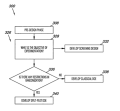
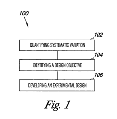
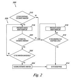
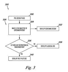
High throughput research workflow
PatentInactiveUS20110029439A1
Innovation
- The method involves quantifying systematic variation through variance component analysis, identifying design objectives, and developing experimental designs such as screening, split-plot, or classical designs to account for systematic variation, and modifying sources of variation to achieve statistically defensible results, using computer-readable mediums and computing devices to implement these steps.
Policy Impact Assessment
High-throughput experimentation (HTE) has emerged as a transformative force in semiconductor research and development, significantly influencing national policy frameworks across major semiconductor-producing nations. The integration of HTE methodologies into national semiconductor strategies has catalyzed a shift in how governments approach industry support, research funding allocation, and international collaboration initiatives.
In the United States, the CHIPS and Science Act represents a direct policy response to the capabilities enabled by HTE, with approximately 15% of its $52.7 billion allocation specifically targeting advanced research facilities equipped with high-throughput capabilities. This policy shift acknowledges that accelerated materials discovery through HTE creates a competitive advantage in semiconductor innovation cycles, reducing time-to-market for next-generation technologies.
The European Union's Chips Act similarly incorporates HTE considerations, establishing dedicated funding streams for pilot facilities that leverage high-throughput methodologies. Policy analysts have noted that this represents a 40% increase in emphasis on experimental throughput compared to previous European semiconductor initiatives, reflecting a growing recognition of HTE's strategic importance.
In East Asia, Japan's semiconductor resilience strategy has been recalibrated to prioritize HTE infrastructure, with recent policy amendments allocating an additional ¥50 billion specifically for high-throughput research platforms. South Korea has implemented tax incentives that provide up to 25% reduction in corporate taxation for semiconductor firms that demonstrate integration of HTE methodologies in their R&D processes.
The policy impact extends beyond funding allocations to regulatory frameworks. Several nations have modified intellectual property policies to address the unique challenges posed by HTE-generated innovations, including specialized patent examination tracks for discoveries made through automated experimentation platforms. These regulatory adaptations reflect the need for policy frameworks to evolve alongside technological capabilities.
International trade policies have also been influenced by HTE capabilities, with export control regulations increasingly focusing on high-throughput equipment and associated technologies. This has created new dimensions in technology transfer restrictions and international scientific collaboration agreements, particularly between competing semiconductor ecosystems.
The workforce development component of national semiconductor policies has similarly evolved in response to HTE adoption, with educational initiatives increasingly emphasizing interdisciplinary training that combines materials science, data analytics, and automation engineering – the core competencies required for effective HTE implementation.
National Security Implications
The integration of High-Throughput Experimentation (HTE) into semiconductor development has profound implications for national security frameworks worldwide. As nations increasingly recognize semiconductors as critical infrastructure, the acceleration of research capabilities through HTE directly impacts strategic defense postures and technological sovereignty. Countries with advanced HTE capabilities gain significant advantages in developing next-generation semiconductor technologies that power military systems, intelligence platforms, and critical infrastructure protection mechanisms.
The security implications extend beyond military applications into economic security domains. Nations lacking robust semiconductor manufacturing capabilities face increased vulnerability to supply chain disruptions, whether from geopolitical tensions, natural disasters, or deliberate interference by adversarial states. HTE's ability to rapidly prototype and test semiconductor materials creates asymmetric advantages for nations that have mastered these techniques, potentially widening the technological gap between leading and developing nations.
Semiconductor supply chain security has emerged as a paramount concern, with HTE serving as both a solution and a challenge. While it enables domestic innovation and potentially reduces dependence on foreign suppliers, it also creates new vectors for intellectual property theft and industrial espionage. Advanced HTE facilities represent high-value intelligence targets, necessitating robust cybersecurity and counterintelligence measures to protect proprietary research methodologies and findings.
The dual-use nature of semiconductor technologies developed through HTE presents complex export control challenges. Technologies that accelerate civilian semiconductor development can simultaneously enhance military capabilities, creating difficult policy decisions regarding international collaboration and technology transfer. Nations must balance innovation through open scientific exchange against the risks of enabling adversaries to develop advanced military applications.
Talent security has become increasingly intertwined with national security in the semiconductor sector. Countries with sophisticated HTE capabilities must implement policies to retain specialized researchers while preventing knowledge transfer that could compromise strategic advantages. This has led to more restrictive visa policies for researchers in sensitive fields and increased scrutiny of international research collaborations involving semiconductor technologies.
As quantum computing and artificial intelligence applications in semiconductor design accelerate through HTE methodologies, new security paradigms are emerging. Nations that successfully leverage HTE to develop quantum-resistant cryptography and AI-enhanced cybersecurity systems will gain significant advantages in protecting critical national infrastructure and sensitive communications networks, reshaping traditional security dynamics in the digital domain.
Unlock deeper insights with Patsnap Eureka Quick Research — get a full tech report to explore trends and direct your research. Try now!
Generate Your Research Report Instantly with AI Agent
Supercharge your innovation with Patsnap Eureka AI Agent Platform!