

Nickel Molybdenum Alloy Offshore Material: Comprehensive Analysis Of Corrosion Resistance, Mechanical Properties, And Marine Applications
JUL 16, 20259 MIN READ
Generate Your Research Report Instantly with AI Agent
PatSnap Eureka helps you evaluate technical feasibility & market potential.
Chiplet Architecture Evolution and Objectives
Chiplet architecture has emerged as a revolutionary approach in the semiconductor industry, evolving from traditional monolithic designs to address the increasing demands of data center applications. This architectural paradigm shift aims to overcome the limitations of conventional chip manufacturing processes, particularly in terms of latency reduction and overall system performance enhancement.
The evolution of chiplet architecture can be traced back to the early 2010s when semiconductor companies began exploring modular chip designs to combat the slowing pace of Moore's Law. As transistor scaling became more challenging and expensive, chiplets offered a viable alternative by allowing the integration of multiple smaller dies onto a single package. This approach enabled the combination of different process nodes and specialized functionalities, leading to improved performance and cost-effectiveness.
The primary objective of chiplet architecture in data centers is to minimize latency while maximizing computational power and energy efficiency. By breaking down complex systems into smaller, more manageable components, chiplets allow for optimized interconnects and reduced signal travel distances. This modular approach facilitates the integration of high-bandwidth memory (HBM) closer to processing units, significantly reducing data access times and improving overall system responsiveness.
Another key goal of chiplet architecture is to enhance scalability and flexibility in data center infrastructure. As workloads become increasingly diverse and demanding, the ability to mix and match different chiplets allows for customized solutions tailored to specific application requirements. This modularity also enables easier upgrades and maintenance, as individual components can be replaced or updated without overhauling the entire system.
The evolution of chiplet architecture has been marked by several significant milestones. The introduction of AMD's Infinity Fabric in 2017 demonstrated the potential of high-speed chip-to-chip interconnects, paving the way for more advanced chiplet designs. Intel's subsequent adoption of chiplet technology with their Foveros 3D packaging further validated the approach, showcasing its potential for vertical integration and improved thermal management.
Looking ahead, the objectives of chiplet architecture in data centers continue to expand. Researchers and industry leaders are focusing on developing standardized interfaces and protocols to facilitate interoperability between chiplets from different manufacturers. This standardization effort aims to create a more diverse and competitive ecosystem, driving innovation and reducing costs across the industry.
Data Center Latency Reduction Demand
The demand for latency reduction in data centers has become increasingly critical as the volume and complexity of data processing continue to grow exponentially. With the rise of cloud computing, artificial intelligence, and big data analytics, data centers are under immense pressure to deliver faster and more efficient services. Latency, which refers to the delay between a request for data and its delivery, has a significant impact on user experience and overall system performance.
In modern data centers, even milliseconds of latency can result in substantial financial losses and decreased user satisfaction. For instance, in high-frequency trading, where split-second decisions can make or break deals, ultra-low latency is paramount. Similarly, in real-time applications such as online gaming, video streaming, and virtual reality, any noticeable delay can severely degrade the user experience.
The increasing adoption of edge computing and the Internet of Things (IoT) has further amplified the need for reduced latency. As more devices connect to the network and generate vast amounts of data, processing this information quickly and efficiently becomes crucial. Edge computing brings data processing closer to the source, reducing the distance data needs to travel and, consequently, the latency.
Moreover, the emergence of 5G networks has set new expectations for low-latency communications. As 5G promises to deliver ultra-low latency for mobile applications, data centers must keep pace to ensure seamless integration and performance across the entire digital ecosystem.
The demand for reduced latency also stems from the need for improved energy efficiency in data centers. Lower latency often correlates with reduced power consumption, as data spends less time in transit and requires fewer resources for processing. This aligns with the growing focus on sustainability and green computing initiatives within the tech industry.
As businesses increasingly rely on real-time analytics and decision-making processes, the pressure on data centers to minimize latency continues to mount. This demand drives innovation in hardware architecture, network design, and software optimization techniques. Chiplet architecture, with its potential to reduce latency through more efficient data processing and communication pathways, emerges as a promising solution to address these pressing needs in modern data center environments.
Chiplet Technology Current State and Challenges
Chiplet technology has emerged as a promising solution to address the challenges of traditional monolithic chip designs in data centers. The current state of chiplet technology is characterized by significant advancements in integration and performance optimization. Leading semiconductor companies have successfully implemented chiplet-based architectures in their high-performance processors, demonstrating improved scalability and reduced manufacturing costs.
One of the primary challenges in chiplet technology is achieving low-latency communication between different chiplets. As data centers demand increasingly faster processing and data transfer speeds, minimizing latency becomes crucial. Current solutions involve advanced packaging technologies such as 2.5D and 3D integration, which allow for closer proximity between chiplets and shorter interconnect lengths.
Another significant challenge is the standardization of chiplet interfaces. While efforts like the Universal Chiplet Interconnect Express (UCIe) consortium are making progress, the industry still lacks a universally adopted standard. This fragmentation can hinder interoperability and limit the potential for mix-and-match chiplet designs across different manufacturers.
Power management and thermal dissipation present additional challenges in chiplet architectures. As multiple chiplets are integrated into a single package, managing power consumption and heat generation becomes more complex. Current solutions include advanced cooling techniques and intelligent power distribution systems, but further innovations are needed to optimize energy efficiency in data center environments.
The geographical distribution of chiplet technology development is primarily concentrated in regions with strong semiconductor industries, such as the United States, Taiwan, and South Korea. However, there is growing interest and investment in chiplet technology across Europe and China as well.
Despite these challenges, chiplet technology continues to advance rapidly. Recent developments include improved die-to-die interconnects, enhanced system-in-package (SiP) designs, and more sophisticated chiplet-aware design tools. These advancements are gradually overcoming the limitations of traditional monolithic designs, particularly in terms of scalability and manufacturing yield.
As the technology matures, researchers and industry leaders are focusing on further reducing inter-chiplet communication latency, improving power efficiency, and enhancing overall system performance. The ultimate goal is to create highly modular, scalable, and efficient chiplet-based architectures that can meet the ever-increasing demands of modern data centers while overcoming the physical limitations of traditional chip designs.
Existing Chiplet Solutions for Latency Reduction
01 Inter-chiplet communication optimization
Techniques to reduce latency in chiplet architectures by optimizing communication between different chiplets. This includes implementing high-speed interconnects, advanced packaging technologies, and efficient data transfer protocols to minimize delays in inter-chiplet communication.- Interconnect optimization for chiplet architecture: Optimizing interconnects between chiplets is crucial for reducing latency in chiplet architectures. This involves designing high-speed, low-latency communication channels between chiplets, implementing advanced packaging technologies, and optimizing the physical layout of chiplets to minimize signal travel distances.
- Memory hierarchy and caching strategies: Implementing efficient memory hierarchies and caching strategies can significantly reduce latency in chiplet architectures. This includes optimizing cache coherence protocols, designing distributed cache systems across chiplets, and implementing intelligent prefetching mechanisms to minimize data access times.
- On-chip network optimization: Optimizing on-chip networks is essential for reducing latency in chiplet architectures. This involves designing efficient network topologies, implementing advanced routing algorithms, and utilizing adaptive link management techniques to minimize congestion and optimize data transfer between chiplets.
- Heterogeneous integration and die stacking: Utilizing heterogeneous integration and die stacking techniques can help reduce latency in chiplet architectures. This includes implementing 2.5D and 3D packaging technologies, optimizing through-silicon via (TSV) designs, and developing advanced bonding techniques to minimize interconnect lengths and improve overall system performance.
- Dynamic voltage and frequency scaling: Implementing dynamic voltage and frequency scaling (DVFS) techniques can help optimize power consumption and reduce latency in chiplet architectures. This involves developing intelligent power management systems that can dynamically adjust voltage and frequency levels of individual chiplets based on workload requirements and thermal constraints.
02 On-chip memory and cache management
Strategies for managing on-chip memory and cache in chiplet architectures to reduce access latency. This involves optimizing memory hierarchies, implementing intelligent caching mechanisms, and utilizing high-bandwidth memory solutions to improve overall system performance.Expand Specific Solutions03 Chiplet-based network-on-chip (NoC) design
Development of efficient network-on-chip architectures specifically tailored for chiplet-based systems. This includes designing low-latency routing algorithms, implementing adaptive network topologies, and optimizing NoC protocols to enhance communication between chiplets.Expand Specific Solutions04 Power management and thermal optimization
Techniques for managing power consumption and thermal characteristics in chiplet architectures to maintain optimal performance and reduce latency. This includes implementing dynamic voltage and frequency scaling, intelligent power gating, and advanced cooling solutions to prevent thermal throttling and maintain low-latency operation.Expand Specific Solutions05 Heterogeneous chiplet integration and synchronization
Methods for integrating and synchronizing heterogeneous chiplets with different functionalities and process technologies. This involves developing efficient interfaces, clock distribution networks, and synchronization mechanisms to minimize latency in cross-chiplet operations and ensure coherent system-level performance.Expand Specific Solutions
Key Players in Chiplet Industry
The chiplet architecture market is in a growth phase, driven by increasing demand for high-performance, low-latency data center solutions. Major players like Intel, AMD, and TSMC are investing heavily in this technology, with the market expected to reach significant size in the coming years. The technology is maturing rapidly, with companies like Micron, SK hynix, and Samsung advancing memory integration. Intel's leadership in chiplet design and AMD's success with their Zen architecture demonstrate the technology's growing maturity. However, challenges in standardization and integration persist, indicating room for further development and innovation in this competitive landscape.
Intel Corp.
Technical Solution: Intel's chiplet architecture, exemplified by their Foveros 3D packaging technology, significantly reduces latency in data centers. This approach allows for the vertical stacking of multiple chiplets, including compute, I/O, and memory dies, within a single package [1]. By bringing these components closer together, signal travel distances are minimized, resulting in lower latency. Intel's implementation includes through-silicon vias (TSVs) and micro-bumps for high-bandwidth, low-latency interconnects between chiplets [2]. Their Ponte Vecchio GPU, designed for data centers and HPC applications, utilizes over 40 chiplets in a single package, demonstrating the scalability of this approach for complex, high-performance systems [3].
Strengths: Highly scalable, allows for mixing of process nodes, and enables more efficient cooling. Weaknesses: Increased manufacturing complexity and potential yield issues with 3D stacking.
QUALCOMM, Inc.
Technical Solution: Qualcomm's approach to chiplet architecture for reducing latency in data centers is exemplified by their work on 5G infrastructure and edge computing solutions. While traditionally focused on mobile technologies, Qualcomm has been expanding into the data center space with their Cloud AI 100 accelerator [11]. This solution utilizes a modular design that can be considered a form of chiplet architecture, optimizing for low-latency AI inference in edge data centers. The company's expertise in system-on-chip (SoC) design translates well to chiplet architectures, allowing for efficient integration of various components like AI accelerators, CPUs, and high-speed interconnects. Qualcomm's focus on power efficiency and high-performance computing at the edge contributes to reduced latency in distributed data center environments [12].
Strengths: Strong expertise in power-efficient designs, well-suited for edge computing and 5G integration. Weaknesses: Less established presence in traditional data center markets compared to some competitors.
Core Innovations in Chiplet Architecture
Computing system architecture having efficient bus connections
PatentPendingUS20250201769A1
Innovation
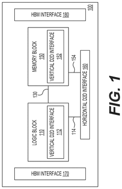
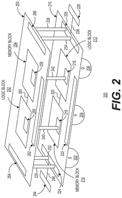
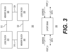
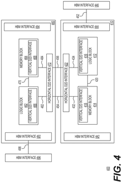
- A computing system architecture that includes a substrate, a memory apparatus, and a host die, where the memory apparatus has multiple memory dies with through vias, and the host die is coupled to the substrate through these vias, enabling efficient data transmission and reducing the need for additional serializer-deserializer (SerDes) circuits.


Homogeneous chiplets configurable as a two-dimensional system or a three-dimensional system
PatentPendingUS20250038120A1
Innovation
- A homogeneous chiplet system is introduced, comprising vertically stacked or horizontally coupled chiplets with on-die interconnect structures and vertical die-to-die interconnection structures, allowing for efficient data signal transfer and reducing latency.
Thermal Management in Chiplet-based Systems
Thermal management is a critical aspect of chiplet-based systems, particularly in data center environments where performance and efficiency are paramount. As chiplet architectures continue to evolve and offer reduced latency in data centers, the challenge of managing heat dissipation becomes increasingly complex. The integration of multiple chiplets within a single package introduces new thermal considerations that must be addressed to ensure optimal system performance and reliability.
One of the primary thermal management strategies in chiplet-based systems involves the use of advanced packaging technologies. These include the implementation of high-performance thermal interface materials (TIMs) between chiplets and heat spreaders, as well as the development of innovative heat spreader designs that efficiently distribute heat across the package. The use of silicon interposers and through-silicon vias (TSVs) also plays a crucial role in facilitating heat transfer between chiplets and the package substrate.
Active cooling solutions are essential for maintaining optimal operating temperatures in chiplet-based systems. Advanced liquid cooling techniques, such as direct liquid cooling and two-phase immersion cooling, are being explored to address the high heat flux generated by densely packed chiplets. These methods offer superior heat dissipation capabilities compared to traditional air cooling approaches, enabling higher performance and improved energy efficiency in data center environments.
The design of chiplet-based systems must also consider thermal-aware floorplanning and power management strategies. By strategically placing chiplets with different power profiles and implementing dynamic power gating techniques, designers can optimize thermal distribution across the package. This approach helps to mitigate hotspots and ensures more uniform heat dissipation, contributing to improved overall system reliability and performance.
Advancements in materials science are driving innovations in thermal management for chiplet-based systems. The development of novel materials with enhanced thermal conductivity properties, such as graphene-based composites and carbon nanotubes, offers promising solutions for improving heat dissipation in future chiplet architectures. These materials have the potential to significantly enhance thermal performance while maintaining the compact form factor required for high-density data center applications.
As chiplet architectures continue to evolve, the integration of on-chip thermal sensors and intelligent thermal management algorithms becomes increasingly important. These technologies enable real-time monitoring and dynamic adjustment of system parameters to optimize thermal performance and power efficiency. By leveraging machine learning techniques, advanced thermal management systems can predict and proactively address potential thermal issues, ensuring consistent performance and reliability in data center environments.
Standardization Efforts in Chiplet Technology
Standardization efforts in chiplet technology are crucial for ensuring interoperability and widespread adoption across the industry. The development of common interfaces and protocols is essential for enabling seamless integration of chiplets from different manufacturers, ultimately reducing latency in data centers.
One of the most significant standardization initiatives is the Universal Chiplet Interconnect Express (UCIe) consortium. Formed by industry leaders such as Intel, AMD, Arm, and TSMC, UCIe aims to establish a universal interconnect standard for chiplets. This standard defines the physical and protocol layers for die-to-die interconnection, facilitating high-bandwidth, low-latency communication between chiplets.
The UCIe specification covers various aspects of chiplet interconnection, including electrical and physical interfaces, protocols, and testing methodologies. By providing a common framework, UCIe enables chiplet designers to focus on their core competencies while ensuring compatibility with other chiplets in the ecosystem.
Another important standardization effort is the Open Compute Project (OCP) Chiplet Design Exchange (CDX) working group. This initiative focuses on developing open standards for chiplet-based designs, including reference architectures, design methodologies, and verification processes. The CDX working group aims to accelerate the adoption of chiplet technology by reducing design complexity and improving time-to-market for chiplet-based products.
The JEDEC Solid State Technology Association has also been actively involved in chiplet standardization. Their JC-63 Committee for Multichip Packages is working on developing standards for chiplet packaging and interconnects, addressing issues such as thermal management, signal integrity, and power delivery.
In addition to these industry-wide efforts, individual companies are also contributing to standardization through open-source initiatives. For example, AMD's Infinity Fabric interconnect technology has been made available to the broader industry, promoting interoperability and fostering innovation in chiplet-based designs.
Standardization efforts extend beyond interconnect technologies to encompass design tools and methodologies. The Electronic System Design Alliance (ESD Alliance) is working on developing standard formats for representing chiplet-based designs, enabling seamless collaboration between different design teams and tools.
As chiplet technology continues to evolve, these standardization efforts will play a crucial role in reducing latency in data centers. By establishing common interfaces and protocols, chiplet-based designs can achieve higher levels of integration and performance, ultimately leading to more efficient and responsive data center architectures.
Unlock deeper insights with PatSnap Eureka Quick Research — get a full tech report to explore trends and direct your research. Try now!
Generate Your Research Report Instantly with AI Agent
Supercharge your innovation with PatSnap Eureka AI Agent Platform!