

How Chiplet Components Secure Next-Level Device Innovations?
JUL 16, 20259 MIN READ
Generate Your Research Report Instantly with AI Agent
PatSnap Eureka helps you evaluate technical feasibility & market potential.
Chiplet Technology Evolution and Objectives
Chiplet technology has emerged as a revolutionary approach in semiconductor design and manufacturing, offering a paradigm shift in how complex integrated circuits are developed. The evolution of chiplets can be traced back to the early 2010s when the limitations of traditional monolithic chip designs became increasingly apparent. As Moore's Law began to slow down, chiplets presented a viable solution to continue advancing computing power and efficiency.
The primary objective of chiplet technology is to overcome the scaling challenges faced by monolithic chip designs. By disaggregating complex system-on-chip (SoC) designs into smaller, more manageable components, chiplets enable the integration of diverse technologies and manufacturing processes within a single package. This approach aims to enhance performance, reduce costs, and improve yield rates in semiconductor production.
One of the key drivers behind chiplet adoption is the need for heterogeneous integration. As different components of a chip often require different process nodes for optimal performance and cost-effectiveness, chiplets allow manufacturers to mix and match the best technologies for each function. This flexibility is crucial for next-level device innovations, particularly in areas such as high-performance computing, artificial intelligence, and 5G communications.
The evolution of chiplet technology has been marked by several significant milestones. Initially, the focus was on developing standardized interfaces and protocols to enable seamless communication between different chiplets. This led to the creation of industry standards such as the Advanced Interface Bus (AIB) and Universal Chiplet Interconnect Express (UCIe), which have been instrumental in fostering interoperability and accelerating chiplet adoption across the industry.
Another critical aspect of chiplet evolution has been the advancement in packaging technologies. Innovations in 2.5D and 3D packaging have made it possible to stack multiple chiplets vertically, significantly increasing the density and performance of semiconductor devices. These packaging advancements have been crucial in realizing the full potential of chiplet-based designs.
Looking ahead, the objectives of chiplet technology are multifaceted. One primary goal is to further improve energy efficiency and performance scaling, which is becoming increasingly challenging with traditional monolithic designs. Chiplets also aim to reduce time-to-market for new products by allowing manufacturers to reuse and recombine existing chiplet designs, thereby accelerating innovation cycles in the semiconductor industry.
Additionally, chiplet technology seeks to democratize access to advanced semiconductor capabilities. By enabling smaller companies to focus on developing specialized chiplets rather than entire SoCs, the technology has the potential to foster greater innovation and competition in the semiconductor ecosystem. This aligns with the broader objective of creating more resilient and diverse supply chains in the global semiconductor industry.
Market Demand for Advanced Device Innovations
The market demand for advanced device innovations is experiencing unprecedented growth, driven by the relentless pursuit of enhanced performance, energy efficiency, and functionality across various sectors. As traditional monolithic chip designs approach their physical limits, the industry is increasingly turning to chiplet technology as a promising solution to meet these evolving demands.
Consumer electronics, particularly smartphones, tablets, and wearables, represent a significant driver for chiplet-based innovations. Users expect devices with longer battery life, faster processing speeds, and more sophisticated features, all within compact form factors. Chiplet technology enables manufacturers to integrate diverse components optimally, addressing these multifaceted requirements while maintaining or even reducing device size.
In the data center and cloud computing sector, the demand for high-performance, energy-efficient servers is skyrocketing. With the exponential growth of data and the proliferation of AI and machine learning applications, there is an urgent need for computing solutions that can handle complex workloads while minimizing power consumption. Chiplet-based designs offer the flexibility to combine high-performance cores with specialized accelerators, meeting the diverse needs of modern data centers.
The automotive industry is another key market driving demand for advanced device innovations. As vehicles become increasingly connected and autonomous, there is a growing need for sophisticated in-vehicle computing systems. These systems must process vast amounts of sensor data in real-time, manage vehicle functions, and ensure passenger safety. Chiplet technology allows for the integration of various specialized processors and sensors, enabling the development of more capable and efficient automotive computing platforms.
In the telecommunications sector, the rollout of 5G networks and the anticipated transition to 6G are creating demand for advanced radio frequency (RF) and signal processing components. Chiplet-based designs can integrate RF, analog, and digital components more effectively, supporting the development of compact, high-performance base stations and mobile devices capable of handling the increased bandwidth and lower latency requirements of next-generation networks.
The industrial and IoT sectors are also fueling demand for chiplet-based innovations. As factories become smarter and more automated, there is a growing need for edge computing devices that can process data locally, reducing latency and improving real-time decision-making. Chiplet technology enables the creation of modular, scalable computing solutions that can be tailored to specific industrial applications, from process control to predictive maintenance.
Chiplet Integration Challenges and Limitations
While chiplets offer significant advantages in device innovation, their integration presents several challenges and limitations that must be addressed for successful implementation. One of the primary challenges is the interconnect technology required to link multiple chiplets effectively. Traditional packaging methods may not provide the necessary bandwidth, latency, or power efficiency for high-performance chiplet-based systems.
The design and manufacturing complexity of chiplet-based systems pose another significant challenge. Integrating multiple chiplets from different process nodes or manufacturers requires sophisticated design tools and methodologies. This complexity can lead to increased development time and costs, potentially offsetting some of the benefits of chiplet technology.
Thermal management is a critical concern in chiplet integration. As chiplets are packed closely together, heat dissipation becomes more challenging, potentially impacting system performance and reliability. Innovative cooling solutions and thermal design considerations are necessary to address this limitation.
Signal integrity and power delivery are also major hurdles in chiplet integration. As signals traverse between chiplets, maintaining signal quality becomes increasingly difficult, especially at high frequencies. Similarly, delivering consistent power across multiple chiplets can be challenging, requiring advanced power distribution networks.
Standardization remains a significant limitation in the chiplet ecosystem. The lack of universal standards for chiplet interfaces and protocols can hinder interoperability between chiplets from different vendors, limiting design flexibility and potentially increasing costs.
Testing and validation of chiplet-based systems present unique challenges. Traditional testing methods may not be sufficient for complex multi-chiplet designs, necessitating new approaches to ensure system reliability and performance.
Yield management in chiplet production and integration is another critical challenge. While chiplets can improve overall yield by allowing the use of smaller die sizes, the integration process itself can introduce yield issues, potentially offsetting some of the benefits.
Finally, the supply chain complexity associated with chiplet-based designs can be a limitation. Coordinating multiple suppliers for different chiplets and ensuring consistent quality and availability can be more challenging than traditional monolithic chip production.
Addressing these challenges and limitations is crucial for realizing the full potential of chiplet technology in driving next-level device innovations. Ongoing research and development efforts are focused on overcoming these hurdles to enable more widespread adoption of chiplet-based designs across various applications and industries.
Current Chiplet Integration Solutions
01 Chiplet interconnection and integration
Innovations in chiplet technology focus on improving interconnection and integration methods between multiple chiplets. This includes advanced packaging techniques, high-bandwidth interfaces, and novel die-to-die communication protocols to enhance overall system performance and efficiency.- Advanced Chiplet Interconnect Technologies: Innovations in chiplet interconnect technologies focus on improving communication between different chiplets within a package. These advancements include high-speed interfaces, novel packaging techniques, and efficient data transfer protocols to enhance overall system performance and reduce latency in multi-chiplet designs.
- Thermal Management Solutions for Chiplet Designs: Developing effective thermal management solutions for chiplet-based devices is crucial. This includes innovative cooling techniques, heat dissipation methods, and thermal interface materials specifically designed for chiplet architectures to maintain optimal operating temperatures and ensure reliability.
- Chiplet Integration and Packaging Innovations: Advancements in chiplet integration and packaging focus on developing new methods for combining multiple chiplets into a single package. This includes 3D stacking technologies, interposer designs, and novel bonding techniques to achieve higher performance, lower power consumption, and reduced form factors.
- Power Management and Distribution for Chiplet Systems: Innovations in power management and distribution for chiplet-based devices aim to optimize energy efficiency and performance. This includes developing advanced power delivery networks, voltage regulation techniques, and power gating strategies tailored for multi-chiplet architectures.
- Chiplet-based AI and Machine Learning Accelerators: Development of specialized chiplets for AI and machine learning applications focuses on creating modular, scalable architectures. These innovations include designing high-performance neural processing units, optimizing data flow between chiplets, and implementing efficient memory hierarchies to accelerate AI workloads.
02 Thermal management for chiplet-based devices
Advancements in thermal management solutions specifically designed for chiplet-based devices. These innovations address the unique cooling challenges posed by densely packed chiplets, including heat spreading techniques, integrated cooling systems, and thermal interface materials optimized for multi-die packages.Expand Specific Solutions03 Power distribution and management in chiplet designs
Novel approaches to power distribution and management in chiplet-based systems. This includes innovations in on-chip power delivery networks, voltage regulation techniques, and power-aware chiplet communication protocols to optimize energy efficiency and performance across multiple dies.Expand Specific Solutions04 Chiplet-based memory and storage solutions
Innovative memory and storage architectures leveraging chiplet technology. These solutions include high-bandwidth memory (HBM) integration, disaggregated memory systems, and novel cache hierarchies designed to work efficiently with chiplet-based processors and accelerators.Expand Specific Solutions05 Heterogeneous integration of chiplets
Advancements in heterogeneous integration of chiplets, combining different process nodes, materials, and functionalities within a single package. This includes innovations in 2.5D and 3D integration techniques, interposer technologies, and chiplet-based system-in-package (SiP) designs for improved performance and functionality.Expand Specific Solutions
Key Players in Chiplet Technology Ecosystem
The chiplet components market is in a dynamic growth phase, driven by increasing demand for advanced device innovations across various sectors. The market is experiencing rapid expansion, with major players like Intel, TSMC, and Samsung Electronics leading the charge. These companies are investing heavily in chiplet technology to enhance performance, reduce costs, and improve energy efficiency. The market's maturity is still evolving, with ongoing research and development efforts from companies such as Micron Technology and Renesas Electronics pushing the boundaries of chiplet integration. As the technology continues to mature, we can expect to see wider adoption across the semiconductor industry, potentially reshaping the landscape of device manufacturing and design.
Micron Technology, Inc.
Technical Solution: Micron's approach to chiplet technology focuses on advanced memory solutions and their integration with compute elements. The company is developing High Bandwidth Memory (HBM) solutions that can be integrated with logic chiplets using 2.5D and 3D packaging technologies[10]. Micron's 3D NAND technology, which stacks multiple layers of memory cells vertically, can be considered a form of chiplet integration within the memory domain[11]. The company is also exploring heterogeneous memory integration, combining different types of memory (e.g., DRAM and NAND) in a single package to optimize performance and capacity for specific applications[12].
Strengths: Expertise in memory technologies and their integration. Potential for optimized memory-compute solutions. Weaknesses: Limited experience in logic chip design compared to some competitors. Dependency on partnerships for full system integration.
Samsung Electronics Co., Ltd.
Technical Solution: Samsung's chiplet approach leverages its advanced packaging technologies, including 2.5D and 3D integration solutions. The company's X-Cube (eXtended-Cube) technology enables the stacking of SRAM or logic dies on top of a base logic die using thousands of TSVs (Through-Silicon Vias)[7]. This approach allows for increased memory bandwidth and reduced power consumption. Samsung is also developing advanced interposer technologies, such as silicon interposers and glass substrates, to facilitate high-bandwidth connections between chiplets[8]. The company's research focuses on improving interconnect density and reducing parasitic effects to enhance overall system performance[9].
Strengths: Vertical integration capabilities from chip design to manufacturing. Advanced memory technologies complement logic integration. Weaknesses: Potential challenges in thermal management for 3D stacked solutions. Complexity in optimizing heterogeneous integration.
Core Innovations in Chiplet Design and Fabrication
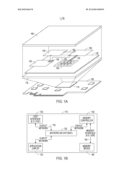
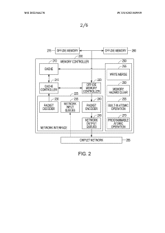
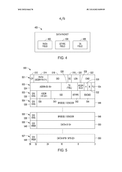
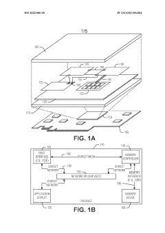
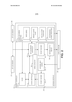
Ordered delivery of data packets based on type of path information in each packet
PatentWO2022046278A1
Innovation
- Incorporating a bridge-type field in data packets to indicate the type of path information, allowing for both address-based and transaction identifier-based ordering, enabling the network to support multiple use cases and bridge between different standards or protocols.
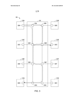
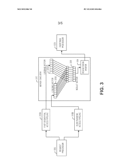
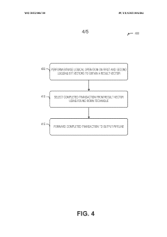
Asynchronous pipeline merging using long vector arbitration
PatentWO2022086730A1
Innovation
- The implementation of long vector arbitration using bitwise operations to represent transactions across parallel paths, allowing for asynchronous and independent completion logging, and a round-robin arbiter to ensure fair handling of completed transactions, thereby maintaining pipeline integrity and throughput.
Standardization Efforts in Chiplet Technology
Standardization efforts in chiplet technology are crucial for ensuring interoperability and fostering innovation across the semiconductor industry. The development of common interfaces and protocols is essential for enabling seamless integration of chiplets from different manufacturers, thereby accelerating the adoption of this modular approach to chip design.
One of the most significant standardization initiatives in the chiplet space is the Universal Chiplet Interconnect Express (UCIe) consortium. Formed by industry leaders such as Intel, AMD, Arm, and TSMC, UCIe aims to establish a universal interconnect standard for chiplets. This standard defines the physical and protocol layers for die-to-die interconnection, allowing for mix-and-match chiplet designs from various vendors.
Another important standardization effort is the Open Compute Project's (OCP) Chiplet Design Exchange (CDX) format. CDX provides a standardized way to describe chiplet designs, facilitating easier exchange of chiplet intellectual property (IP) between different companies and design teams. This standardization helps streamline the chiplet ecosystem and promotes collaboration among industry players.
The JEDEC Solid State Technology Association has also been active in chiplet standardization, particularly in the area of memory interfaces. Their efforts include the development of standards for High Bandwidth Memory (HBM) and other memory technologies that can be integrated as chiplets in advanced system-in-package (SiP) designs.
Standardization efforts extend to packaging technologies as well. The Heterogeneous Integration Roadmap (HIR), sponsored by IEEE, SEMI, and other organizations, provides a comprehensive view of the challenges and potential solutions for integrating diverse chiplets into a single package. This roadmap helps align industry efforts and guide research and development activities.
The adoption of these standards is critical for enabling a robust chiplet ecosystem. By providing a common framework for chiplet design and integration, these standards reduce barriers to entry for smaller companies and accelerate innovation across the industry. They also help address challenges related to thermal management, power delivery, and signal integrity in multi-chiplet designs.
As chiplet technology continues to evolve, ongoing standardization efforts will play a vital role in shaping the future of semiconductor design and manufacturing. These initiatives will be key to unlocking the full potential of chiplet-based architectures and securing next-level device innovations across a wide range of applications, from high-performance computing to mobile devices and IoT systems.
Economic Impact of Chiplet Adoption
The adoption of chiplet technology is poised to have a significant economic impact across the semiconductor industry and beyond. As traditional monolithic chip designs reach their physical and economic limits, chiplets offer a more flexible and cost-effective approach to semiconductor manufacturing. This shift is expected to drive down production costs while simultaneously enabling more powerful and efficient devices.
One of the primary economic benefits of chiplet adoption is the potential for improved yield rates in semiconductor manufacturing. By breaking down complex chip designs into smaller, more manageable components, manufacturers can reduce the likelihood of defects and increase overall production efficiency. This improvement in yield rates translates directly to cost savings, as fewer chips need to be discarded due to manufacturing errors.
Furthermore, chiplets allow for greater flexibility in product design and customization. Companies can mix and match different chiplet components to create a wide range of products tailored to specific market needs. This modularity reduces development costs and time-to-market for new devices, enabling companies to respond more quickly to changing consumer demands and technological advancements.
The chiplet approach also has the potential to democratize the semiconductor industry by lowering barriers to entry. Smaller companies and startups can focus on developing specialized chiplets rather than entire system-on-chip (SoC) designs, fostering innovation and competition in the market. This diversification of the supply chain could lead to a more resilient and dynamic semiconductor ecosystem.
From a broader economic perspective, the adoption of chiplet technology is expected to drive growth in various sectors that rely on advanced computing capabilities. Industries such as artificial intelligence, autonomous vehicles, and 5G telecommunications stand to benefit from the increased performance and efficiency offered by chiplet-based devices. This technological advancement could spur new business opportunities and contribute to overall economic growth.
However, the transition to chiplet-based designs is not without challenges. Significant investments in research, development, and manufacturing infrastructure will be required to fully realize the potential of this technology. Companies that successfully navigate this transition are likely to gain a competitive edge in the market, while those that lag behind may face economic pressures.
In conclusion, the economic impact of chiplet adoption is expected to be far-reaching, reshaping the semiconductor industry and influencing various sectors of the global economy. As this technology matures and becomes more widespread, it has the potential to drive innovation, reduce costs, and create new opportunities for businesses and consumers alike.
Unlock deeper insights with PatSnap Eureka Quick Research — get a full tech report to explore trends and direct your research. Try now!
Generate Your Research Report Instantly with AI Agent
Supercharge your innovation with PatSnap Eureka AI Agent Platform!