How Chiplet Innovations Support Next-Gen Device Connectivity?
JUL 16, 20259 MIN READ
Generate Your Research Report Instantly with AI Agent
Patsnap Eureka helps you evaluate technical feasibility & market potential.
Chiplet Technology Evolution and Connectivity Goals
Chiplet technology has emerged as a revolutionary approach in semiconductor design and manufacturing, addressing the challenges of traditional monolithic chip architectures. The evolution of chiplets can be traced back to the early 2010s when the industry began exploring modular chip designs to overcome the limitations of Moore's Law. As transistor scaling became increasingly difficult and expensive, chiplets offered a way to continue improving performance and functionality without relying solely on shrinking transistor sizes.
The primary goal of chiplet technology is to enable the creation of more complex and powerful systems-on-chip (SoCs) by combining multiple smaller dies, or chiplets, into a single package. This approach allows for greater flexibility in design, improved yield, and the ability to mix and match different process nodes and technologies within a single device. As connectivity becomes increasingly critical in next-generation devices, chiplet innovations play a crucial role in supporting high-speed, low-latency communication between different components.
One of the key objectives in chiplet technology evolution is to develop advanced packaging techniques that can efficiently integrate multiple chiplets. This includes innovations in interposer technologies, such as silicon and organic interposers, which provide the necessary interconnects between chiplets. Additionally, the development of through-silicon vias (TSVs) and micro-bumps has been instrumental in enabling vertical stacking and high-density connections between chiplets.
Another important goal is the standardization of chiplet interfaces and protocols. Initiatives like the Universal Chiplet Interconnect Express (UCIe) aim to create a common framework for chiplet-to-chiplet communication, promoting interoperability and reducing design complexity. This standardization effort is crucial for fostering a more open ecosystem where chiplets from different vendors can be seamlessly integrated.
As next-generation devices demand ever-increasing bandwidth and lower power consumption, chiplet innovations are focused on developing high-speed, energy-efficient interconnects. This includes advancements in SerDes (Serializer/Deserializer) technology, optical interconnects, and novel materials for improved signal integrity. These innovations are essential for supporting the connectivity requirements of emerging applications such as 5G, artificial intelligence, and high-performance computing.
The evolution of chiplet technology also aims to address thermal management challenges associated with high-performance, densely packed systems. Innovations in cooling solutions, such as integrated liquid cooling and advanced thermal interface materials, are being developed to ensure optimal performance and reliability of chiplet-based devices.
Market Demand for Advanced Device Interconnects
The demand for advanced device interconnects is rapidly growing, driven by the increasing complexity and performance requirements of modern electronic systems. As devices become more sophisticated and data-intensive, traditional interconnect technologies are reaching their limits in terms of bandwidth, power efficiency, and scalability. This has created a significant market opportunity for innovative chiplet-based solutions that can address these challenges.
In the consumer electronics sector, there is a strong demand for high-speed, low-latency interconnects to support next-generation smartphones, tablets, and wearable devices. These products require seamless connectivity between various components, such as processors, memory, and sensors, to deliver enhanced user experiences and support emerging applications like augmented reality and artificial intelligence.
The data center and cloud computing markets are also driving demand for advanced interconnects. With the exponential growth of data traffic and the need for more powerful servers, there is a critical requirement for interconnect technologies that can handle massive data throughput while minimizing power consumption and heat generation. Chiplet-based solutions offer the potential to meet these demands by enabling modular, scalable architectures that can be optimized for specific workloads.
In the automotive industry, the shift towards autonomous vehicles and advanced driver assistance systems (ADAS) is creating a need for high-performance, reliable interconnects. These systems require real-time processing of vast amounts of sensor data, necessitating robust and efficient communication between various electronic components within the vehicle.
The telecommunications sector, particularly with the rollout of 5G networks, is another key driver of demand for advanced interconnects. As network infrastructure evolves to support higher data rates and lower latency, there is a growing need for interconnect technologies that can handle the increased bandwidth requirements while maintaining signal integrity over longer distances.
Industrial IoT and edge computing applications are also contributing to the market demand for advanced interconnects. These use cases often require distributed processing capabilities and real-time data analysis, creating a need for efficient communication between sensors, processors, and other components in challenging environmental conditions.
The market for advanced device interconnects is expected to continue growing as emerging technologies such as artificial intelligence, machine learning, and quantum computing gain traction. These fields require unprecedented levels of computational power and data movement, further driving the need for innovative interconnect solutions that can overcome current limitations and support future technological advancements.
Current Challenges in Chiplet-based Connectivity
Chiplet-based connectivity faces several significant challenges in the current technological landscape. One of the primary issues is the complexity of inter-chiplet communication. As chiplets are essentially separate dies integrated onto a single package, ensuring seamless and efficient data transfer between these components is crucial. The interconnect technology used for this purpose must support high bandwidth, low latency, and low power consumption, which is a delicate balance to achieve.
Another challenge lies in the standardization of chiplet interfaces. The lack of universal standards for chiplet-to-chiplet communication protocols hinders interoperability and limits the potential for mix-and-match chiplet designs from different vendors. This fragmentation in the industry slows down innovation and increases development costs, as companies must invest in proprietary solutions or adapt to multiple interface standards.
Thermal management presents a significant hurdle in chiplet-based designs. As more chiplets are integrated into a single package, the power density increases, leading to potential hotspots and overall thermal challenges. Efficient heat dissipation becomes critical to maintain performance and reliability, requiring advanced cooling solutions and thermal-aware design strategies.
Signal integrity and power delivery are also major concerns in chiplet-based connectivity. As signals traverse between chiplets, they are susceptible to degradation due to factors such as crosstalk, electromagnetic interference, and impedance mismatches. Ensuring clean signal transmission across the interposer or substrate is essential for maintaining data integrity at high speeds. Similarly, delivering stable power to each chiplet while managing voltage drops and current fluctuations across the package is a complex task.
Manufacturing and testing pose unique challenges for chiplet-based designs. The assembly process for multi-chiplet packages requires precise alignment and bonding techniques. Additionally, testing individual chiplets before integration and then testing the assembled package introduces new complexities in the quality assurance process. Developing effective test methodologies for chiplet-based systems is crucial for ensuring reliability and yield.
Lastly, the design and simulation tools for chiplet-based systems are still evolving. Traditional EDA tools are often not optimized for the unique requirements of chiplet designs, such as modeling inter-chiplet interactions or optimizing system-level performance across multiple dies. This gap in design tools can lead to longer development cycles and potential oversights in system optimization.
Existing Chiplet Connectivity Solutions
01 Interconnect technologies for chiplet integration
Various interconnect technologies are employed to facilitate communication between chiplets in multi-chip modules. These may include advanced packaging techniques, high-speed serial links, and novel interconnect architectures designed to optimize data transfer between chiplets while minimizing latency and power consumption.- Interconnect technologies for chiplet integration: Various interconnect technologies are used to enable communication between chiplets in multi-chip modules. These may include advanced packaging techniques, high-speed interfaces, and novel interconnect architectures to facilitate efficient data transfer between chiplets. The focus is on reducing latency, increasing bandwidth, and improving overall system performance.
- 3D integration and stacking for chiplet connectivity: Three-dimensional integration and stacking techniques are employed to enhance chiplet connectivity. This approach involves vertically stacking chiplets using through-silicon vias (TSVs) or other advanced packaging methods. It allows for shorter interconnects, higher density, and improved thermal management in chiplet-based designs.
- Network-on-Chip (NoC) architectures for chiplet communication: Network-on-Chip architectures are utilized to facilitate communication between chiplets. These architectures provide scalable and flexible interconnect solutions, allowing for efficient data routing and reduced congestion in complex chiplet-based systems. NoC designs can be optimized for specific chiplet configurations and application requirements.
- Power management and distribution in chiplet systems: Effective power management and distribution strategies are crucial for chiplet connectivity. This includes techniques for optimizing power delivery to individual chiplets, managing thermal issues, and implementing power-aware communication protocols. The goal is to ensure reliable operation and maximize energy efficiency in chiplet-based designs.
- Standardization and interoperability in chiplet interfaces: Efforts are being made to standardize chiplet interfaces and promote interoperability between chiplets from different vendors. This includes developing common protocols, electrical specifications, and physical interfaces to enable seamless integration of diverse chiplets. Standardization aims to foster a more open and flexible ecosystem for chiplet-based system design.
02 3D stacking and through-silicon vias (TSVs) for chiplet connectivity
3D stacking techniques and through-silicon vias (TSVs) are utilized to create vertical connections between chiplets, enabling higher bandwidth, reduced footprint, and improved thermal management in chiplet-based designs. This approach allows for more efficient use of silicon area and enhanced overall system performance.Expand Specific Solutions03 Chiplet-to-chiplet communication protocols and interfaces
Specialized communication protocols and interfaces are developed to facilitate efficient data exchange between chiplets. These may include custom bus architectures, packetized communication schemes, and standardized interfaces designed to ensure compatibility and interoperability between chiplets from different vendors or manufacturing processes.Expand Specific Solutions04 Power management and distribution for chiplet-based systems
Innovative power management and distribution techniques are implemented to address the unique challenges of chiplet-based designs. This includes strategies for efficient power delivery to individual chiplets, voltage regulation, and thermal management to ensure optimal performance and reliability of the overall system.Expand Specific Solutions05 Packaging and assembly methods for chiplet integration
Advanced packaging and assembly methods are developed to enable effective integration of multiple chiplets into a single package. These techniques may involve novel substrate technologies, die-to-die bonding approaches, and innovative heat dissipation solutions to ensure reliable connectivity and performance in chiplet-based systems.Expand Specific Solutions
Key Players in Chiplet and Interconnect Industry
The chiplet innovation landscape is evolving rapidly, with major players like Intel, Micron, and Huawei driving advancements in next-gen device connectivity. The industry is in a growth phase, with increasing market size as chiplet technology matures and finds applications in various sectors. Companies are at different stages of technological maturity, with established semiconductor giants like Intel and Qualcomm leading in R&D and product development. Emerging players such as AvicenaTech and Primemas are introducing innovative solutions, while research institutions like Zhejiang Lab contribute to foundational advancements. The competitive landscape is dynamic, with collaborations and partnerships forming to address complex integration challenges and drive standardization efforts.
Micron Technology, Inc.
Technical Solution: Micron's contribution to chiplet innovation primarily focuses on memory solutions. They have developed High Bandwidth Memory (HBM) stacks, which can be considered as memory chiplets, designed to be integrated with processors or other logic chips using 2.5D or 3D packaging technologies[10]. Micron has also been working on their Hybrid Memory Cube (HMC) technology, which uses Through-Silicon Vias (TSVs) to stack multiple DRAM dies, creating high-bandwidth, low-latency memory solutions that can be closely integrated with processors[11]. Their latest developments include research into compute-in-memory architectures, where memory chiplets incorporate some computational capabilities, potentially revolutionizing data-intensive applications[12].
Strengths: Expertise in memory technologies, potential for high-bandwidth and low-latency memory solutions. Weaknesses: Limited scope outside of memory applications, dependence on partnerships for full system integration.
Huawei Technologies Co., Ltd.
Technical Solution: Huawei has been actively developing chiplet technologies as part of their efforts to enhance their semiconductor capabilities. Their approach includes the development of a chiplet-based architecture for their Kirin mobile SoCs, allowing for more flexible integration of various IP blocks[13]. Huawei has also invested in advanced packaging technologies, including fan-out wafer-level packaging (FOWLP) and through-silicon via (TSV) interconnects, to support high-bandwidth connections between chiplets[14]. The company has been exploring the use of 2.5D and 3D packaging techniques to integrate heterogeneous chiplets, including AI accelerators and custom logic, alongside their main SoC designs[15]. Despite facing challenges due to trade restrictions, Huawei continues to innovate in chiplet technologies to maintain competitiveness in the mobile and 5G markets.
Strengths: Strong integration capabilities, expertise in mobile and 5G technologies. Weaknesses: Geopolitical challenges affecting access to advanced manufacturing technologies, potential limitations in scaling production.
Core Innovations in Chiplet Interconnect Technologies
Edge interface placements to enable chiplet rotation into multi-chiplet cluster
PatentPendingUS20240332257A1
Innovation
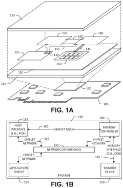
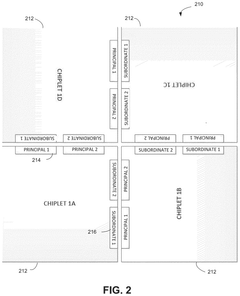
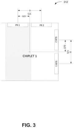
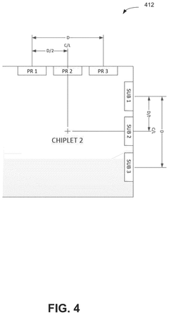
- The implementation of a chiplet architecture that uses a network-on-chip (NOC) with a chiplet protocol interface (CPI) to facilitate high-speed, flexible inter-chiplet communication, combined with a tightly packed matrix arrangement of chiplets and I/O micro-bumps for close-coupled interconnects, allowing for proper alignment and minimal footprint.
Chiplet Optical Interconnection System, Data Transmission Method, Device, Equipment and Medium
PatentPendingCN120263285A
Innovation
- The optical interconnection system of the core particle is adopted, and the optical transmitting module and the optical receiving module switch in the connection state of the chip-level optical base is realized, and the optical switching nodes and optical waveguide network are used to route and topological control of the optical signal.


Standardization Efforts in Chiplet Interfaces
Standardization efforts in chiplet interfaces have become a crucial aspect of advancing next-generation device connectivity. As the semiconductor industry moves towards disaggregated chip designs, the need for common standards to ensure interoperability and seamless integration has become paramount.
Several industry consortia and organizations have emerged to address this challenge. The Universal Chiplet Interconnect Express (UCIe) consortium, formed in 2022, has been at the forefront of developing open standards for die-to-die interconnects. UCIe aims to create a unified ecosystem that enables chiplets from different vendors to work together seamlessly, fostering innovation and reducing time-to-market for new products.
Another significant initiative is the Open Compute Project's (OCP) Chiplet Design Exchange (CDX) working group. This group focuses on developing standards for chiplet-based designs, including physical and logical interfaces, as well as design methodologies. Their efforts complement those of UCIe by addressing broader aspects of chiplet integration.
The JEDEC Solid State Technology Association has also been active in this space, working on standards for high-bandwidth memory (HBM) interfaces and other chiplet-related technologies. Their JC-42 committee has been instrumental in developing specifications for memory interfaces that are critical for chiplet-based systems.
In parallel, the IEEE has been developing standards such as IEEE 2851, which aims to create a unified standard for 2.5D and 3D multi-die interconnects. This standard addresses the need for consistent methodologies in designing and verifying complex multi-die systems.
These standardization efforts are not without challenges. One of the primary hurdles is balancing the need for a common standard with the desire for proprietary innovations that provide competitive advantages. Companies must navigate the fine line between collaboration and competition, ensuring that standards are open enough to foster widespread adoption while still allowing for differentiation.
Another challenge lies in the rapid pace of technological advancement in the chiplet space. Standards must be flexible enough to accommodate future innovations while providing a stable foundation for current designs. This requires a delicate balance and continuous updates to the standards as technology evolves.
Despite these challenges, the benefits of standardization are clear. Common interfaces and protocols can significantly reduce design complexity, lower costs, and accelerate time-to-market for new products. They also enable a more diverse and competitive ecosystem, allowing smaller players to innovate alongside industry giants.
As chiplet technology continues to mature, these standardization efforts will play a crucial role in shaping the future of device connectivity. The success of these initiatives will be measured by their ability to foster innovation, promote interoperability, and drive the adoption of chiplet-based designs across the semiconductor industry.
Energy Efficiency in Chiplet Interconnects
Energy efficiency in chiplet interconnects has become a critical focus in the development of next-generation device connectivity. As chiplet technology continues to evolve, the need for more efficient and high-performance interconnects has grown exponentially. Traditional monolithic chip designs face limitations in terms of power consumption and heat dissipation, making chiplet-based architectures an attractive alternative for addressing these challenges.
One of the primary advantages of chiplet interconnects is their ability to optimize power usage across different functional units. By separating various components into individual chiplets, designers can implement targeted power management strategies for each module. This granular approach allows for more precise control over energy consumption, enabling the system to allocate power resources more efficiently based on workload demands.
Advanced packaging technologies play a crucial role in enhancing the energy efficiency of chiplet interconnects. Through the use of 2.5D and 3D integration techniques, manufacturers can reduce the physical distance between chiplets, minimizing signal loss and power consumption associated with data transmission. These packaging innovations also facilitate the implementation of high-bandwidth, low-power interconnect solutions such as silicon interposers and through-silicon vias (TSVs).
The development of specialized interconnect protocols has further contributed to improving energy efficiency in chiplet-based systems. Industry standards like Universal Chiplet Interconnect Express (UCIe) and Advanced Interface Bus (AIB) have been designed to optimize data transfer between chiplets while minimizing power consumption. These protocols incorporate features such as low-voltage signaling, power-aware link training, and dynamic frequency scaling to reduce energy usage during both active and idle states.
Emerging technologies in the field of chiplet interconnects are pushing the boundaries of energy efficiency even further. Photonic interconnects, for instance, offer the potential for ultra-low power consumption and high-bandwidth data transfer between chiplets. By leveraging light-based communication, these interconnects can significantly reduce the energy required for data transmission compared to traditional electrical interconnects.
As the demand for more powerful and energy-efficient devices continues to grow, the focus on optimizing chiplet interconnects will remain at the forefront of semiconductor innovation. The ongoing research and development in this area promise to deliver increasingly sophisticated solutions that balance performance requirements with the critical need for energy conservation in next-generation computing systems.
Unlock deeper insights with Patsnap Eureka Quick Research — get a full tech report to explore trends and direct your research. Try now!
Generate Your Research Report Instantly with AI Agent
Supercharge your innovation with Patsnap Eureka AI Agent Platform!