

How EUV Lithography Supports Artificial Intelligence Hardware Growth
OCT 14, 20259 MIN READ
Generate Your Research Report Instantly with AI Agent
PatSnap Eureka helps you evaluate technical feasibility & market potential.
EUV Lithography Evolution and AI Hardware Goals
Extreme Ultraviolet (EUV) lithography represents a revolutionary advancement in semiconductor manufacturing technology, marking a significant departure from traditional Deep Ultraviolet (DUV) lithography methods. Since its conceptualization in the 1980s, EUV lithography has evolved from theoretical research to commercial implementation, overcoming numerous technical challenges along the way. The technology utilizes 13.5nm wavelength light to achieve unprecedented precision in semiconductor fabrication, enabling the production of increasingly smaller transistors and more complex integrated circuits.
The evolution of EUV lithography has been characterized by several key milestones. Initially, researchers faced significant hurdles in developing suitable light sources, mirrors, and photoresist materials capable of working with such short wavelengths. By the early 2010s, companies like ASML had developed the first viable EUV lithography systems, though throughput and reliability remained concerns. Recent years have seen dramatic improvements in these areas, with modern EUV systems achieving the production volumes necessary for commercial viability.
This technological progression aligns perfectly with the exponential growth in computational demands driven by artificial intelligence applications. AI hardware development faces increasing pressure to deliver higher performance, greater energy efficiency, and enhanced computational density. These requirements necessitate more sophisticated chip designs with smaller feature sizes and higher transistor counts—precisely what EUV lithography enables.
The primary technical goal of EUV lithography in the context of AI hardware is to continue scaling semiconductor devices according to Moore's Law, which has been increasingly challenged using traditional lithography techniques. By enabling feature sizes below 7nm, down to 3nm and potentially beyond, EUV lithography provides the foundation for developing specialized AI accelerators, neural processing units, and high-bandwidth memory systems that form the backbone of modern AI infrastructure.
Additionally, EUV technology aims to support the development of heterogeneous integration and 3D chip stacking, which are becoming essential for AI hardware architectures. These approaches allow for optimized combinations of processing elements, memory subsystems, and interconnects that can be tailored specifically for AI workloads such as training large language models or performing real-time inference at the edge.
Looking forward, the continued evolution of EUV lithography will focus on enabling high-volume manufacturing at even smaller nodes (2nm and below), improving yield rates, and reducing costs per wafer. These advancements will be crucial for meeting the projected exponential growth in AI computational requirements, which are doubling approximately every 3-4 months for leading-edge models, far outpacing the traditional 18-24 month doubling period described by Moore's Law.
The evolution of EUV lithography has been characterized by several key milestones. Initially, researchers faced significant hurdles in developing suitable light sources, mirrors, and photoresist materials capable of working with such short wavelengths. By the early 2010s, companies like ASML had developed the first viable EUV lithography systems, though throughput and reliability remained concerns. Recent years have seen dramatic improvements in these areas, with modern EUV systems achieving the production volumes necessary for commercial viability.
This technological progression aligns perfectly with the exponential growth in computational demands driven by artificial intelligence applications. AI hardware development faces increasing pressure to deliver higher performance, greater energy efficiency, and enhanced computational density. These requirements necessitate more sophisticated chip designs with smaller feature sizes and higher transistor counts—precisely what EUV lithography enables.
The primary technical goal of EUV lithography in the context of AI hardware is to continue scaling semiconductor devices according to Moore's Law, which has been increasingly challenged using traditional lithography techniques. By enabling feature sizes below 7nm, down to 3nm and potentially beyond, EUV lithography provides the foundation for developing specialized AI accelerators, neural processing units, and high-bandwidth memory systems that form the backbone of modern AI infrastructure.
Additionally, EUV technology aims to support the development of heterogeneous integration and 3D chip stacking, which are becoming essential for AI hardware architectures. These approaches allow for optimized combinations of processing elements, memory subsystems, and interconnects that can be tailored specifically for AI workloads such as training large language models or performing real-time inference at the edge.
Looking forward, the continued evolution of EUV lithography will focus on enabling high-volume manufacturing at even smaller nodes (2nm and below), improving yield rates, and reducing costs per wafer. These advancements will be crucial for meeting the projected exponential growth in AI computational requirements, which are doubling approximately every 3-4 months for leading-edge models, far outpacing the traditional 18-24 month doubling period described by Moore's Law.
Market Demand for Advanced Semiconductor Manufacturing
The semiconductor manufacturing market is experiencing unprecedented demand driven by the rapid advancement of artificial intelligence technologies. This surge is particularly evident in the need for high-performance AI chips that require increasingly sophisticated manufacturing processes. EUV (Extreme Ultraviolet) lithography has emerged as a critical enabler for producing the advanced semiconductors that power AI systems, creating a symbiotic relationship between semiconductor manufacturing capabilities and AI hardware evolution.
Market research indicates that the global AI chip market is projected to grow at a compound annual growth rate of over 30% through 2027, significantly outpacing the broader semiconductor industry. This growth is fueled by data centers, autonomous vehicles, smartphones, and emerging edge computing applications that all require increasingly powerful AI processing capabilities. These applications demand chips with higher transistor densities, greater computational efficiency, and lower power consumption – specifications that can only be achieved through advanced manufacturing processes like EUV lithography.
The demand for EUV-enabled semiconductor manufacturing is further amplified by the exponential growth in AI model complexity. As AI models like large language models (LLMs) continue to scale, they require exponentially more computational power. For instance, training advanced AI models can require hundreds of petaflops of computing power, necessitating specialized AI accelerators manufactured using the most advanced process nodes.
Leading cloud service providers and AI companies are investing heavily in custom silicon solutions optimized for AI workloads. These companies are competing to secure manufacturing capacity at leading foundries that utilize EUV lithography, creating a competitive landscape where access to advanced semiconductor manufacturing capabilities has become a strategic advantage. This has resulted in multi-billion dollar investments in semiconductor manufacturing infrastructure globally.
Regional dynamics are also shaping market demand, with governments worldwide recognizing advanced semiconductor manufacturing as a strategic national priority. The CHIPS Act in the United States, the European Chips Act, and similar initiatives in Asia represent significant public investments aimed at expanding domestic advanced semiconductor manufacturing capabilities, with particular emphasis on supporting AI hardware development.
The economic impact extends beyond the semiconductor industry itself. Industries adopting AI solutions – from healthcare to automotive to financial services – are creating derivative demand for advanced chips. This multiplier effect further intensifies the market pressure for expanded EUV lithography capacity and continued innovation in semiconductor manufacturing processes.
Supply constraints in the EUV lithography equipment market have created additional market dynamics, with ASML – the sole supplier of production-grade EUV lithography systems – facing backorders extending multiple years. This supply limitation has become a critical factor in strategic planning for semiconductor manufacturers and their AI hardware customers, influencing investment decisions and technology roadmaps across the industry.
Market research indicates that the global AI chip market is projected to grow at a compound annual growth rate of over 30% through 2027, significantly outpacing the broader semiconductor industry. This growth is fueled by data centers, autonomous vehicles, smartphones, and emerging edge computing applications that all require increasingly powerful AI processing capabilities. These applications demand chips with higher transistor densities, greater computational efficiency, and lower power consumption – specifications that can only be achieved through advanced manufacturing processes like EUV lithography.
The demand for EUV-enabled semiconductor manufacturing is further amplified by the exponential growth in AI model complexity. As AI models like large language models (LLMs) continue to scale, they require exponentially more computational power. For instance, training advanced AI models can require hundreds of petaflops of computing power, necessitating specialized AI accelerators manufactured using the most advanced process nodes.
Leading cloud service providers and AI companies are investing heavily in custom silicon solutions optimized for AI workloads. These companies are competing to secure manufacturing capacity at leading foundries that utilize EUV lithography, creating a competitive landscape where access to advanced semiconductor manufacturing capabilities has become a strategic advantage. This has resulted in multi-billion dollar investments in semiconductor manufacturing infrastructure globally.
Regional dynamics are also shaping market demand, with governments worldwide recognizing advanced semiconductor manufacturing as a strategic national priority. The CHIPS Act in the United States, the European Chips Act, and similar initiatives in Asia represent significant public investments aimed at expanding domestic advanced semiconductor manufacturing capabilities, with particular emphasis on supporting AI hardware development.
The economic impact extends beyond the semiconductor industry itself. Industries adopting AI solutions – from healthcare to automotive to financial services – are creating derivative demand for advanced chips. This multiplier effect further intensifies the market pressure for expanded EUV lithography capacity and continued innovation in semiconductor manufacturing processes.
Supply constraints in the EUV lithography equipment market have created additional market dynamics, with ASML – the sole supplier of production-grade EUV lithography systems – facing backorders extending multiple years. This supply limitation has become a critical factor in strategic planning for semiconductor manufacturers and their AI hardware customers, influencing investment decisions and technology roadmaps across the industry.
EUV Technology Status and Implementation Challenges
Extreme Ultraviolet (EUV) lithography represents a significant technological breakthrough in semiconductor manufacturing, currently deployed primarily by industry leaders such as TSMC, Samsung, and Intel. The technology operates at a 13.5nm wavelength, enabling the production of chips with feature sizes below 7nm, which is critical for advanced AI hardware development. Despite its transformative potential, EUV implementation faces substantial challenges that impact its broader adoption across the semiconductor industry.
The most significant technical challenge remains the EUV light source stability and power. Current systems typically operate at 250-300 watts, but achieving consistent output power while maintaining minimal downtime continues to be problematic. This directly impacts throughput and cost-effectiveness, especially when considering the demands of AI chip production which requires both precision and scale.
Mask defectivity presents another major hurdle. EUV masks are fundamentally different from traditional optical masks, utilizing reflective rather than transmissive technology. The complexity of manufacturing defect-free masks and inspecting them efficiently remains a significant technical constraint, with defects as small as 10nm potentially causing critical failures in AI processor architectures.
Photoresist performance also presents unique challenges in the EUV domain. The interaction between EUV photons and resist materials differs fundamentally from traditional lithography, requiring specialized chemistries that can deliver high resolution, sensitivity, and line-edge roughness control simultaneously. This "triangle of death" trade-off becomes particularly critical for AI hardware, where pattern fidelity directly impacts computational performance.
From a manufacturing perspective, EUV lithography systems represent extraordinary capital investments, with each tool costing approximately $150-200 million. This economic barrier restricts access to only the largest semiconductor manufacturers, creating potential bottlenecks in the AI hardware supply chain. Additionally, the complex integration of EUV into existing fabrication workflows requires substantial facility modifications and specialized expertise.
Geographically, EUV technology development remains concentrated in specific regions. ASML (Netherlands) maintains a monopoly on EUV system manufacturing, while key components come from specialized suppliers primarily in Europe, Japan, and the United States. This concentration creates potential supply chain vulnerabilities for the global AI hardware ecosystem.
Energy consumption presents another significant challenge, with EUV systems requiring 10-20 times more power than previous lithography technologies. This increased energy footprint raises concerns about sustainability as AI hardware production scales up to meet growing computational demands.
The most significant technical challenge remains the EUV light source stability and power. Current systems typically operate at 250-300 watts, but achieving consistent output power while maintaining minimal downtime continues to be problematic. This directly impacts throughput and cost-effectiveness, especially when considering the demands of AI chip production which requires both precision and scale.
Mask defectivity presents another major hurdle. EUV masks are fundamentally different from traditional optical masks, utilizing reflective rather than transmissive technology. The complexity of manufacturing defect-free masks and inspecting them efficiently remains a significant technical constraint, with defects as small as 10nm potentially causing critical failures in AI processor architectures.
Photoresist performance also presents unique challenges in the EUV domain. The interaction between EUV photons and resist materials differs fundamentally from traditional lithography, requiring specialized chemistries that can deliver high resolution, sensitivity, and line-edge roughness control simultaneously. This "triangle of death" trade-off becomes particularly critical for AI hardware, where pattern fidelity directly impacts computational performance.
From a manufacturing perspective, EUV lithography systems represent extraordinary capital investments, with each tool costing approximately $150-200 million. This economic barrier restricts access to only the largest semiconductor manufacturers, creating potential bottlenecks in the AI hardware supply chain. Additionally, the complex integration of EUV into existing fabrication workflows requires substantial facility modifications and specialized expertise.
Geographically, EUV technology development remains concentrated in specific regions. ASML (Netherlands) maintains a monopoly on EUV system manufacturing, while key components come from specialized suppliers primarily in Europe, Japan, and the United States. This concentration creates potential supply chain vulnerabilities for the global AI hardware ecosystem.
Energy consumption presents another significant challenge, with EUV systems requiring 10-20 times more power than previous lithography technologies. This increased energy footprint raises concerns about sustainability as AI hardware production scales up to meet growing computational demands.
Current EUV Solutions for AI Chip Production
01 EUV Lithography System Components
Extreme Ultraviolet (EUV) lithography systems consist of specialized components designed to work with short-wavelength light. These systems include EUV light sources, reflective optics (as traditional transmissive optics absorb EUV radiation), specialized masks, and precise positioning stages. The integration of these components enables the creation of semiconductor devices with feature sizes below 10nm, representing a significant advancement in lithography technology.- EUV Lithography System Design and Components: EUV lithography systems incorporate specialized components designed to work with extreme ultraviolet light. These systems typically include radiation sources, illumination optics, reticle stages, projection optics, and wafer stages. The design focuses on maintaining precise alignment and stability while operating in vacuum conditions required for EUV wavelengths. Advanced control systems manage thermal effects and vibration to ensure nanometer-level accuracy during the lithography process.
- EUV Source Technology and Optimization: EUV radiation sources typically use laser-produced plasma or discharge-produced plasma to generate the extreme ultraviolet light needed for lithography. These sources involve striking tin, xenon or other target materials with lasers or electrical discharges to create high-energy plasma that emits EUV radiation. Innovations focus on increasing source power, stability, and conversion efficiency while reducing debris generation that can contaminate optical components. Collector optics and debris mitigation systems are critical components for maintaining consistent EUV output.
- EUV Mask and Reticle Technology: EUV masks consist of multilayer reflective coatings on substrates with absorber patterns that define circuit features. Unlike traditional transmissive photomasks, EUV masks operate by reflection due to the strong absorption of EUV wavelengths by most materials. Innovations include defect inspection and repair techniques, pattern enhancement features, and protective pellicles to prevent contamination. Advanced mask designs incorporate phase-shifting elements and assist features to improve image fidelity and process windows for critical dimensions at extreme scales.
- EUV Resist Materials and Processing: Photoresist materials for EUV lithography are specially formulated to be highly sensitive to EUV radiation while maintaining high resolution and low line edge roughness. These materials typically employ chemical amplification mechanisms where a single photon can trigger multiple chemical reactions. Innovations focus on increasing sensitivity to reduce required exposure doses, improving pattern fidelity, and developing processing techniques that minimize defects. Post-exposure bake processes and development chemistries are optimized to work with the unique exposure characteristics of EUV radiation.
- EUV Optical Systems and Contamination Control: EUV optical systems use specialized multilayer mirrors that can reflect extreme ultraviolet light at specific angles. These optical components require extraordinary precision in manufacturing and positioning to maintain wavefront quality. Contamination control is critical as carbon and other contaminants can rapidly degrade mirror reflectivity. Systems incorporate sophisticated environmental controls, including vacuum systems, hydrogen purging, and in-situ cleaning technologies. Advanced metrology systems continuously monitor optical performance and compensate for degradation to maintain consistent imaging quality throughout production runs.
02 EUV Source Technology
EUV light sources are critical components that generate the extreme ultraviolet radiation needed for lithography. These sources typically use laser-produced plasma or discharge-produced plasma techniques to create EUV radiation at 13.5nm wavelength. The development of high-power, stable EUV sources has been essential for making EUV lithography commercially viable, as they must provide sufficient power while maintaining spectral purity and minimal debris generation.Expand Specific Solutions03 EUV Mask Technology
EUV masks differ significantly from traditional photomasks as they operate in reflection rather than transmission mode. These masks consist of multilayer reflective coatings with patterned absorber layers. The development of defect-free masks is crucial for EUV lithography, as even nanometer-scale defects can cause critical pattern failures. Advanced inspection and repair technologies have been developed specifically for EUV mask manufacturing and maintenance.Expand Specific Solutions04 EUV Process Control and Optimization
Controlling the EUV lithography process requires sophisticated metrology and optimization techniques. This includes precise dose control, focus management, and overlay accuracy. Advanced computational methods are employed to predict and compensate for process variations. Additionally, specialized resist materials have been developed to enhance sensitivity to EUV radiation while maintaining the resolution and line edge roughness requirements for advanced semiconductor nodes.Expand Specific Solutions05 EUV Integration with Semiconductor Manufacturing
Integrating EUV lithography into semiconductor manufacturing workflows presents unique challenges. This includes developing compatible process steps before and after EUV exposure, managing thermal effects, and ensuring contamination control. Specialized vacuum systems and handling equipment are required due to the absorption of EUV radiation by air. The integration also involves optimizing the overall manufacturing process to maximize the benefits of EUV's high resolution while managing its cost and throughput limitations.Expand Specific Solutions
Key EUV Equipment Manufacturers and Chip Producers
The EUV lithography market is experiencing rapid growth driven by AI hardware demands, currently in an accelerated expansion phase. Market size is projected to reach billions as AI chip production increases, requiring advanced semiconductor manufacturing capabilities. Technology maturity varies among key players: ASML Netherlands BV dominates with its monopoly on EUV lithography systems, while Taiwan Semiconductor Manufacturing Co. (TSMC) and Samsung Electronics lead in implementation. Supporting ecosystem players include Shin-Etsu Chemical and AGC providing specialized materials, with Synopsys offering design tools. Chinese entities like SMIC and research institutions are working to close the technological gap, though Western companies maintain significant advantages in this critical AI-enabling technology.
Taiwan Semiconductor Manufacturing Co., Ltd.
Technical Solution: TSMC has pioneered the implementation of ASML's EUV lithography technology in high-volume manufacturing, becoming the first foundry to mass-produce 7nm and 5nm chips using EUV processes. Their N5 (5nm) and N3 (3nm) process nodes heavily leverage EUV lithography to create the dense, power-efficient transistor architectures required for AI accelerators and neural processing units. TSMC has developed specialized design rules and process optimizations specifically for AI chip manufacturing using EUV, enabling customers like NVIDIA, AMD, and Google to produce their AI accelerator chips with unprecedented computational density. Their CoWoS (Chip-on-Wafer-on-Substrate) advanced packaging technology complements EUV lithography by allowing heterogeneous integration of multiple AI processing dies with high-bandwidth memory, critical for large language models and deep learning applications[2]. TSMC has reported that their EUV-based processes deliver up to 80% higher logic density and 20% power reduction compared to previous generation technologies, directly translating to AI chips that can process more parameters with greater energy efficiency[4]. Their 3nm process node uses up to 30+ EUV layers and enables neural network accelerators with over 100 billion transistors.
Strengths: Industry-leading implementation of EUV in high-volume manufacturing; comprehensive AI chip ecosystem from design to production; advanced packaging technologies that complement EUV lithography for complete AI solutions. Weaknesses: High capital expenditure requirements for maintaining technology leadership; geopolitical vulnerabilities due to concentration of advanced manufacturing; capacity constraints during periods of high AI chip demand.
ASML Netherlands BV
Technical Solution: ASML is the dominant player in EUV lithography technology, holding over 90% market share in this critical semiconductor manufacturing equipment. Their NXE series EUV lithography systems, particularly the NXE:3600D, achieve resolution down to 13nm with a numerical aperture of 0.33, enabling the production of 3nm and 5nm node chips essential for AI accelerators. ASML's EUV technology utilizes a 13.5nm wavelength light source generated by converting droplets of molten tin into plasma using high-powered CO2 lasers. This process creates the extreme ultraviolet light needed to pattern the intricate circuits on silicon wafers that power advanced AI processors. Their systems incorporate sophisticated computational lithography techniques and machine learning algorithms to optimize pattern fidelity and yield, directly supporting the manufacturing of high-performance AI chips with greater transistor density and energy efficiency[1][3]. ASML's High-NA EUV technology (0.55 NA) is under development to enable even smaller features below 10nm, critical for future AI hardware that requires increasingly complex neural network architectures.
Strengths: Unrivaled market dominance and technological leadership in EUV lithography; continuous innovation pipeline with High-NA EUV development; comprehensive ecosystem of partners and suppliers. Weaknesses: Extremely high system costs (>$150 million per tool) limiting accessibility; complex supply chain vulnerabilities; significant energy consumption requirements for EUV light generation.
Critical Patents and Innovations in EUV Technology
Extreme ultraviolet photolithography method
PatentActiveUS20200413526A1
Innovation
- Integration of a gas flow mechanism with the collector, including a gas supply module and exhaust system, to remove debris, combined with a shroud and shutter cover design to stabilize metallic droplet trajectories and shield against shock waves, thereby reducing contamination and maintaining the collector's reflectivity.


Mask Stitching for Extreme Ultraviolet Lithography
PatentPendingUS20250199397A1
Innovation
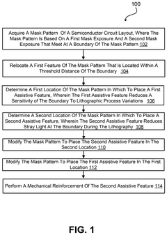
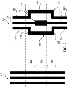
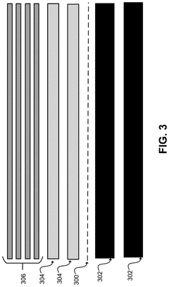
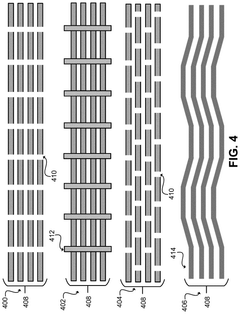
- The method involves determining locations within the mask pattern to place assistive features that reduce sensitivity to lithographic process variations and stray light at the boundary during mask exposures. These assistive features are strategically placed to mitigate the effects of double exposure in the boundary region.
Supply Chain Resilience for EUV Equipment
The resilience of the EUV lithography equipment supply chain represents a critical factor in sustaining artificial intelligence hardware development. ASML's near-monopoly position as the sole manufacturer of EUV lithography machines creates a significant vulnerability in the semiconductor ecosystem that powers AI advancement. This concentration risk is amplified by the extraordinary complexity of EUV systems, which contain over 100,000 parts sourced from multiple countries and suppliers.
The COVID-19 pandemic exposed the fragility of this supply chain, causing delays in EUV equipment delivery that subsequently impacted advanced chip production schedules for AI accelerators and processors. These disruptions highlighted the need for strategic redundancy in critical component sourcing. Currently, key optical components, particularly the specialized mirrors required for EUV systems, are manufactured by a limited number of suppliers, creating potential bottlenecks.
Geopolitical tensions have further complicated supply chain management for EUV equipment. Export controls and trade restrictions between major economies have created uncertainty regarding access to critical technologies and components. The strategic importance of EUV lithography for national security and technological leadership has elevated these tools to the status of geopolitical assets, requiring careful navigation of international regulations.
To enhance resilience, leading semiconductor manufacturers are implementing several strategies. Long-term procurement agreements with ASML have become standard practice, with companies like TSMC, Samsung, and Intel securing multi-year commitments for EUV systems. Additionally, strategic inventory management of critical spare parts and consumables helps mitigate short-term supply disruptions that could otherwise halt AI chip production.
Vertical integration efforts are also emerging, with some semiconductor manufacturers investing in capabilities to produce certain components internally or forming joint ventures with suppliers. This approach reduces dependency on external vendors for the most critical elements. Simultaneously, geographical diversification of the supply base is being pursued where technically feasible, though the specialized nature of many EUV components limits this strategy's effectiveness.
Looking forward, industry consortia and public-private partnerships are forming to address supply chain vulnerabilities collectively. These initiatives focus on developing alternative sourcing options, standardizing certain components, and investing in next-generation manufacturing capabilities that could eventually support a more distributed production model for advanced lithography equipment supporting AI hardware development.
The COVID-19 pandemic exposed the fragility of this supply chain, causing delays in EUV equipment delivery that subsequently impacted advanced chip production schedules for AI accelerators and processors. These disruptions highlighted the need for strategic redundancy in critical component sourcing. Currently, key optical components, particularly the specialized mirrors required for EUV systems, are manufactured by a limited number of suppliers, creating potential bottlenecks.
Geopolitical tensions have further complicated supply chain management for EUV equipment. Export controls and trade restrictions between major economies have created uncertainty regarding access to critical technologies and components. The strategic importance of EUV lithography for national security and technological leadership has elevated these tools to the status of geopolitical assets, requiring careful navigation of international regulations.
To enhance resilience, leading semiconductor manufacturers are implementing several strategies. Long-term procurement agreements with ASML have become standard practice, with companies like TSMC, Samsung, and Intel securing multi-year commitments for EUV systems. Additionally, strategic inventory management of critical spare parts and consumables helps mitigate short-term supply disruptions that could otherwise halt AI chip production.
Vertical integration efforts are also emerging, with some semiconductor manufacturers investing in capabilities to produce certain components internally or forming joint ventures with suppliers. This approach reduces dependency on external vendors for the most critical elements. Simultaneously, geographical diversification of the supply base is being pursued where technically feasible, though the specialized nature of many EUV components limits this strategy's effectiveness.
Looking forward, industry consortia and public-private partnerships are forming to address supply chain vulnerabilities collectively. These initiatives focus on developing alternative sourcing options, standardizing certain components, and investing in next-generation manufacturing capabilities that could eventually support a more distributed production model for advanced lithography equipment supporting AI hardware development.
Environmental Impact of EUV Manufacturing Processes
The environmental footprint of Extreme Ultraviolet (EUV) lithography represents a significant consideration as this technology accelerates AI hardware development. EUV systems consume substantial energy, with each lithography machine requiring approximately 1 megawatt of power during operation—equivalent to the electricity needs of about 800 households. This energy intensity stems from the complex process of generating EUV light, which involves converting droplets of molten tin into plasma using high-powered CO2 lasers.
Water usage presents another environmental challenge, as EUV manufacturing processes demand ultra-pure water for cleaning silicon wafers between production steps. A typical semiconductor fabrication facility utilizing EUV technology can consume 4-5 million gallons of water daily, raising concerns about resource sustainability in regions where these facilities operate.
The production of EUV lithography equipment also involves rare earth elements and specialized materials with environmentally intensive extraction processes. These materials require energy-intensive mining and refining operations that generate significant carbon emissions and potential ecological disruption in source regions.
Chemical usage in EUV processes presents additional environmental considerations. The photoresists and development chemicals employed contain potentially hazardous substances that require careful handling and disposal protocols to prevent environmental contamination. While the semiconductor industry has made progress in reducing the use of perfluorinated compounds and other persistent pollutants, the chemical footprint remains substantial.
Waste management challenges are amplified by EUV's precision requirements. The technology generates specialized waste streams including used photoresists, etching solutions, and equipment components with limited recycling pathways. The semiconductor industry continues to develop more effective recycling and circular economy approaches, though significant challenges remain.
Despite these environmental concerns, EUV lithography offers potential sustainability advantages through efficiency improvements. By enabling more powerful AI chips with lower power requirements per computation, EUV technology contributes to reducing the overall energy consumption of AI systems at scale. Additionally, the industry has begun implementing environmental mitigation strategies, including heat recovery systems, water recycling technologies, and renewable energy integration at fabrication facilities.
As AI hardware demands continue growing exponentially, balancing technological advancement with environmental responsibility will require continued innovation in manufacturing processes, materials science, and facility design to minimize EUV lithography's ecological footprint while supporting the computational needs of next-generation artificial intelligence systems.
Water usage presents another environmental challenge, as EUV manufacturing processes demand ultra-pure water for cleaning silicon wafers between production steps. A typical semiconductor fabrication facility utilizing EUV technology can consume 4-5 million gallons of water daily, raising concerns about resource sustainability in regions where these facilities operate.
The production of EUV lithography equipment also involves rare earth elements and specialized materials with environmentally intensive extraction processes. These materials require energy-intensive mining and refining operations that generate significant carbon emissions and potential ecological disruption in source regions.
Chemical usage in EUV processes presents additional environmental considerations. The photoresists and development chemicals employed contain potentially hazardous substances that require careful handling and disposal protocols to prevent environmental contamination. While the semiconductor industry has made progress in reducing the use of perfluorinated compounds and other persistent pollutants, the chemical footprint remains substantial.
Waste management challenges are amplified by EUV's precision requirements. The technology generates specialized waste streams including used photoresists, etching solutions, and equipment components with limited recycling pathways. The semiconductor industry continues to develop more effective recycling and circular economy approaches, though significant challenges remain.
Despite these environmental concerns, EUV lithography offers potential sustainability advantages through efficiency improvements. By enabling more powerful AI chips with lower power requirements per computation, EUV technology contributes to reducing the overall energy consumption of AI systems at scale. Additionally, the industry has begun implementing environmental mitigation strategies, including heat recovery systems, water recycling technologies, and renewable energy integration at fabrication facilities.
As AI hardware demands continue growing exponentially, balancing technological advancement with environmental responsibility will require continued innovation in manufacturing processes, materials science, and facility design to minimize EUV lithography's ecological footprint while supporting the computational needs of next-generation artificial intelligence systems.
Unlock deeper insights with PatSnap Eureka Quick Research — get a full tech report to explore trends and direct your research. Try now!
Generate Your Research Report Instantly with AI Agent
Supercharge your innovation with PatSnap Eureka AI Agent Platform!