

How to Maximize Data Throughput with Neuromorphic Chips
SEP 8, 202510 MIN READ
Generate Your Research Report Instantly with AI Agent
PatSnap Eureka helps you evaluate technical feasibility & market potential.
Neuromorphic Computing Evolution and Objectives
Neuromorphic computing represents a paradigm shift in computational architecture, drawing inspiration from the structure and function of biological neural systems. The evolution of this field can be traced back to the late 1980s when Carver Mead first introduced the concept of using analog circuits to mimic neurobiological architectures. This pioneering work laid the foundation for what would eventually become a significant branch of computing research aimed at overcoming the limitations of traditional von Neumann architectures.
The development trajectory of neuromorphic computing has been marked by several key milestones. In the 1990s, research primarily focused on analog VLSI implementations of neural systems. The early 2000s saw the emergence of digital neuromorphic systems, which offered improved scalability and integration capabilities. By the 2010s, hybrid analog-digital approaches gained prominence, combining the efficiency of analog computation with the precision and programmability of digital systems.
Recent years have witnessed an acceleration in neuromorphic chip development, driven by the increasing demands of artificial intelligence applications and the approaching physical limits of conventional semiconductor technology. Major research institutions and technology companies have invested heavily in neuromorphic research, resulting in notable implementations such as IBM's TrueNorth, Intel's Loihi, and BrainChip's Akida, each representing different approaches to neuromorphic architecture.
The primary objective of neuromorphic computing is to achieve brain-like efficiency in processing complex, unstructured data. While conventional computing excels at precise, sequential operations, it struggles with the parallel, adaptive processing required for tasks like pattern recognition and sensory processing. Neuromorphic systems aim to bridge this gap by implementing massively parallel architectures with co-located memory and processing elements, significantly reducing the energy consumption and latency associated with data movement.
Specifically regarding data throughput maximization, neuromorphic computing presents unique opportunities and challenges. The inherent parallelism of these systems offers potential for high throughput processing of certain workloads, particularly those involving sparse, event-driven data. However, realizing this potential requires addressing several technical objectives: optimizing spike-based communication protocols, developing efficient neural encoding schemes for conventional data, creating programming models that leverage neuromorphic parallelism, and designing architectures that balance the trade-offs between biological fidelity and engineering practicality.
The evolution of neuromorphic computing is increasingly being shaped by its potential applications in edge computing, where power constraints are significant but real-time processing of sensory data is essential. This application domain has focused development efforts on achieving higher throughput while maintaining the energy efficiency that makes neuromorphic computing attractive in the first place.
Market Demand Analysis for High-Throughput Neural Processing
The neuromorphic computing market is experiencing unprecedented growth, driven by the increasing demand for high-throughput neural processing capabilities across multiple industries. Current market analysis indicates that the global neuromorphic chip market is projected to grow at a compound annual growth rate of 89% through 2028, reflecting the urgent need for more efficient data processing solutions in AI applications.
This explosive growth is primarily fueled by the limitations of traditional computing architectures when handling complex neural network operations. Conventional von Neumann architectures create bottlenecks between memory and processing units, significantly constraining data throughput for neural network applications. Organizations across sectors are actively seeking solutions that can overcome these limitations to process massive datasets more efficiently.
Healthcare represents one of the most promising markets for high-throughput neuromorphic processing. Medical imaging analysis, real-time patient monitoring systems, and drug discovery processes all require processing enormous volumes of complex data with minimal latency. The ability of neuromorphic chips to handle parallel processing while consuming significantly less power makes them ideal for portable medical devices and hospital systems requiring continuous operation.
Autonomous vehicles constitute another critical market segment driving demand for enhanced neural processing capabilities. These systems must process data from multiple sensors simultaneously while making split-second decisions. Current solutions struggle with the power consumption and processing speed requirements, creating a substantial market opportunity for neuromorphic solutions that can deliver higher throughput while operating within strict power constraints.
Edge computing applications represent a rapidly expanding market for neuromorphic processing. As IoT deployments scale, the need to process sensor data locally rather than transmitting it to cloud servers has become paramount. Market research indicates that approximately 75% of enterprise-generated data will be processed at the edge by 2025, creating significant demand for high-throughput, energy-efficient neural processing solutions.
Financial services institutions are increasingly adopting AI for fraud detection, algorithmic trading, and risk assessment. These applications require processing vast transaction datasets in real-time, creating demand for neuromorphic solutions that can deliver superior throughput compared to traditional computing architectures.
Defense and security applications represent another substantial market segment, with requirements for real-time image recognition, signal processing, and threat detection systems that can operate in resource-constrained environments. The ability of neuromorphic chips to deliver high throughput while consuming minimal power makes them particularly attractive for deployment in field operations and unmanned systems.
Current Neuromorphic Chip Architectures and Bottlenecks
Current neuromorphic computing architectures represent a significant departure from traditional von Neumann computing paradigms, drawing inspiration from the structure and function of biological neural systems. The landscape of neuromorphic chip designs is dominated by several key architectures, each with distinct approaches to neural processing and data throughput optimization.
Spiking Neural Network (SNN) based chips, such as IBM's TrueNorth and Intel's Loihi, utilize event-driven processing where information is encoded in the timing and frequency of discrete spikes. While these designs excel in energy efficiency, they face throughput limitations due to the serial nature of spike processing and the challenges in efficiently translating conventional data formats into spike trains.
Memristor-based neuromorphic systems represent another architectural approach, utilizing non-volatile memory elements that can simultaneously store and process information. These systems offer promising density and parallelism advantages but encounter bottlenecks related to device variability, limited precision, and challenges in scaling manufacturing processes to commercial volumes.
Analog computing neuromorphic designs leverage the inherent physics of electronic components to perform neural computations directly in the analog domain. While these systems can achieve remarkable energy efficiency and computational density, they struggle with signal noise, temperature sensitivity, and precision limitations that can constrain reliable high-throughput operations.
Digital neuromorphic implementations provide greater precision and programmability but typically consume more power and silicon area per neural operation compared to their analog counterparts. The primary bottleneck in these systems stems from the fundamental trade-off between flexibility and specialized efficiency.
Interconnect limitations represent a universal bottleneck across all neuromorphic architectures. The dense connectivity patterns required to mimic biological neural networks create significant challenges in chip design, often resulting in communication bottlenecks that limit overall system throughput regardless of the computational efficiency of individual neural elements.
Memory bandwidth constraints further exacerbate throughput limitations, as the massive parallelism potential of neuromorphic systems can only be realized with sufficient memory access capabilities. Current designs struggle to balance on-chip memory capacity with the need for external memory access, creating potential data transfer bottlenecks.
Programming and software ecosystem immaturity also presents significant challenges. The lack of standardized programming models, development tools, and optimization techniques specifically designed for neuromorphic computing creates inefficiencies in how these architectures are utilized, often preventing them from achieving their theoretical throughput potential.
Addressing these architectural bottlenecks requires innovative approaches that span hardware design, materials science, programming paradigms, and system integration strategies to fully unlock the data throughput potential of neuromorphic computing systems.
Current Data Throughput Enhancement Techniques
01 Neuromorphic architecture optimization for data throughput
Neuromorphic chips can be optimized for data throughput by implementing specialized architectures that mimic neural networks. These architectures include parallel processing pathways, optimized memory hierarchies, and dedicated data routing mechanisms that significantly reduce bottlenecks. By organizing computational units in a brain-inspired manner, these chips can process multiple data streams simultaneously, leading to enhanced throughput capabilities while maintaining energy efficiency.- Neuromorphic architecture optimization for data throughput: Neuromorphic chips can be optimized for data throughput by implementing specialized architectures that mimic neural networks. These architectures include parallel processing pathways, optimized memory hierarchies, and dedicated hardware accelerators that enable efficient data flow. By designing chip architectures specifically for neural processing, data throughput can be significantly increased compared to traditional computing approaches, allowing for faster processing of complex neural network operations.
- Spike-based processing for improved data throughput: Spike-based processing in neuromorphic chips enables efficient data throughput by transmitting information only when needed, similar to biological neurons. This approach reduces power consumption while maintaining high processing capabilities. Spike-timing-dependent plasticity (STDP) and other spiking neural network techniques allow for event-driven computation that processes data asynchronously, leading to improved throughput for real-time applications and complex pattern recognition tasks.
- Memory integration for enhanced data throughput: Integrating memory directly within neuromorphic chips significantly enhances data throughput by reducing the bottleneck between processing and memory access. This approach includes in-memory computing, where computations are performed directly within memory arrays, and 3D stacked memory architectures that provide high-bandwidth connections to processing elements. These memory integration techniques minimize data movement, which is traditionally a major limitation in computing performance, resulting in faster and more energy-efficient neural network operations.
- Parallel processing techniques for neuromorphic data throughput: Neuromorphic chips leverage massive parallelism to achieve high data throughput by simultaneously processing multiple neural operations. These techniques include distributed processing across multiple cores, vector processing units specifically designed for neural computations, and specialized interconnect fabrics that enable efficient communication between processing elements. The parallel nature of these chips allows them to handle complex neural network operations with significantly higher throughput than sequential processing approaches.
- Hardware-software co-optimization for throughput enhancement: Maximizing data throughput in neuromorphic chips requires co-optimization of hardware and software components. This includes developing specialized compilers that map neural networks efficiently to the underlying hardware, runtime systems that dynamically allocate resources based on workload characteristics, and hardware-aware training algorithms that consider the physical constraints of the neuromorphic architecture. This holistic approach ensures that the full potential of the neuromorphic hardware is utilized, resulting in optimal data throughput for various neural network applications.
02 Memory integration techniques for improved data flow
Advanced memory integration techniques are crucial for maximizing data throughput in neuromorphic chips. These include on-chip memory structures positioned close to processing elements, specialized cache hierarchies, and novel memory architectures like memristive devices. By reducing the physical distance between computation and storage elements, these approaches minimize data transfer latency and increase overall system throughput, enabling more efficient processing of neural network operations.Expand Specific Solutions03 Spike-based communication protocols for efficient data transfer
Spike-based communication protocols enhance data throughput in neuromorphic systems by transmitting information only when necessary. These event-driven protocols reduce bandwidth requirements by encoding information in the timing and frequency of spikes rather than continuous data streams. This approach allows for efficient communication between neural processing units, optimizing data transfer across the chip and enabling higher throughput for complex neural network applications.Expand Specific Solutions04 Hardware acceleration techniques for neural processing
Hardware acceleration techniques specifically designed for neural processing can significantly improve data throughput in neuromorphic chips. These include specialized circuits for common neural operations, pipelined processing elements, and custom logic for activation functions. By implementing these acceleration techniques at the hardware level, neuromorphic chips can achieve higher throughput rates while processing complex neural network models, enabling real-time applications in areas such as computer vision and natural language processing.Expand Specific Solutions05 Interconnect optimization for neural network data flow
Optimized interconnect architectures are essential for maximizing data throughput in neuromorphic chips. These include hierarchical network-on-chip designs, crossbar arrays, and reconfigurable routing mechanisms that efficiently handle the complex connectivity patterns of neural networks. By implementing these specialized interconnect structures, neuromorphic chips can support the massive parallel data transfers required by neural computations, reducing communication bottlenecks and enhancing overall system throughput.Expand Specific Solutions
Leading Companies and Research Institutions in Neuromorphic Computing
The neuromorphic chip market for maximizing data throughput is currently in its growth phase, with an expanding market size driven by increasing demand for edge AI applications. The technology maturity varies across key players, with companies like Syntiant Corp., IBM, and Huawei leading commercial deployment of ultra-low-power neuromorphic solutions. Academic institutions including Tsinghua University and KAIST are advancing fundamental research, while specialized firms such as Polyn Technology and Grai Matter Labs focus on application-specific implementations. Western Digital and SK Hynix contribute memory expertise critical for throughput optimization. The competitive landscape features both established semiconductor giants and innovative startups, with collaboration between industry and academia accelerating development of more efficient neuromorphic architectures for high-throughput data processing.
Syntiant Corp.
Technical Solution: Syntiant has developed the Neural Decision Processor (NDP) architecture specifically designed to maximize data throughput for edge AI applications. Their approach focuses on ultra-low power neuromorphic computing that can efficiently process sensor data streams. The NDP architecture implements a unique memory-centric design where computation happens directly within memory arrays, dramatically reducing the energy and time costs associated with moving data between separate memory and processing units. This approach enables throughput improvements of up to 100x compared to traditional CPU/GPU architectures for specific workloads. Syntiant's chips utilize a specialized neural network architecture optimized for processing temporal data streams, making them particularly effective for audio and speech applications where continuous high-throughput processing is required. The company has implemented an advanced weight compression technique that reduces memory requirements while maintaining accuracy, allowing for more complex models to be deployed on resource-constrained devices. Their latest generation chips incorporate adaptive power management that dynamically adjusts processing resources based on workload demands, ensuring optimal throughput-to-power ratios across varying operational conditions.
Strengths: Extremely low power consumption (under 1mW) enabling always-on applications; highly optimized for specific workloads like keyword spotting and sensor processing; production-ready solutions with commercial deployment. Weaknesses: More specialized for audio/speech applications rather than general-purpose computing; limited flexibility for adapting to entirely new types of neural network architectures; smaller scale compared to major semiconductor companies.
Polyn Technology Ltd.
Technical Solution: Polyn Technology has developed a Neuromorphic Analog Signal Processing (NASP) platform that takes a unique approach to maximizing data throughput. Their technology combines neuromorphic principles with analog computing to process sensor data directly in the analog domain, eliminating the need for traditional analog-to-digital conversion that often creates bottlenecks in data throughput. The NASP architecture implements a novel approach where incoming analog signals are processed through neuromorphic circuits that perform feature extraction and classification directly on the raw sensor data. This approach reduces latency and increases effective throughput by eliminating preprocessing stages required in conventional digital systems. Polyn's chips utilize a specialized analog memory technology that stores neural network weights as analog values, enabling highly efficient multiply-accumulate operations that form the core of neural network computation. Their architecture incorporates parallel processing pathways optimized for different signal characteristics, allowing simultaneous processing of multiple data streams without throughput degradation. Polyn has also developed adaptive power management techniques that dynamically adjust the precision and power consumption of different processing elements based on the complexity of the incoming data, ensuring optimal throughput-to-power ratios across varying workloads.
Strengths: Direct analog processing eliminates ADC bottlenecks; extremely low power consumption suitable for battery-powered devices; reduced latency compared to digital approaches. Weaknesses: Potential precision limitations inherent to analog computing; more susceptible to manufacturing variations and noise; narrower application focus compared to general-purpose digital solutions.
Breakthrough Patents in Neuromorphic Data Processing
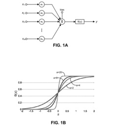
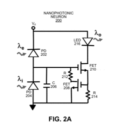
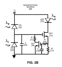
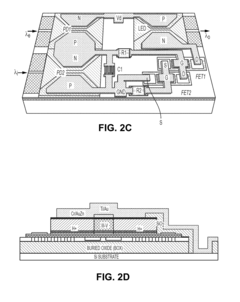
Implementing a neuromorphic computing system using nanophotonic neurons
PatentActiveUS20190065941A1
Innovation
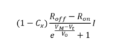
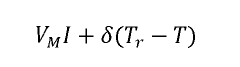
- A photonic neuron system is designed with excitatory and inhibitory input detectors, an electrical neuron for integrating signals, and a light-emitting output device, implemented in a 3D integrated neuromorphic computing system using nanophotonic neural networks and optical interconnection networks with Mach-Zehnder interferometer blocks, enabling efficient energy use and scalability.
Mixed-mode crossbar arrays and associated methods
PatentWO2023049984A1
Innovation
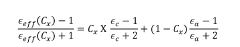
- A mixed-mode crossbar array that integrates optical and electrical interactions using mixed-mode memory elements, which can exhibit persistent states programmable via electrical or optical signals, allowing for both optical and electrical readout, enabling efficient matrix multiplication and neural network training through optical and electrical pathways.

Energy Efficiency vs. Throughput Trade-offs
The fundamental challenge in neuromorphic computing lies in balancing energy efficiency with data throughput capabilities. Neuromorphic chips, designed to mimic brain functionality, inherently offer significant energy advantages over traditional von Neumann architectures. However, maximizing data throughput often requires design decisions that can compromise these efficiency benefits.
Current neuromorphic implementations demonstrate energy consumption as low as picojoules per synaptic operation, representing orders of magnitude improvement over conventional computing systems. This efficiency stems from event-driven processing paradigms where computation occurs only when necessary, eliminating the constant power draw of clock-driven systems. However, when optimizing for maximum throughput, designers often increase operating frequencies and parallel processing capabilities, which directly impacts power consumption.
The trade-off curve between energy efficiency and throughput is non-linear. Research indicates that throughput improvements follow approximately a square root relationship with energy consumption increases. This means doubling throughput typically requires quadrupling energy expenditure, creating diminishing returns as systems scale toward higher performance targets.
Architectural decisions significantly impact this balance. Spike-based communication protocols offer excellent energy characteristics but may limit throughput compared to more traditional digital signaling. Similarly, memory placement relative to processing elements creates another critical trade-off point. Near-memory or in-memory computing reduces data movement costs but increases chip complexity and potentially reduces maximum operating frequencies.
Recent innovations have focused on hybrid approaches that dynamically adjust the energy-throughput balance based on workload characteristics. These systems implement multiple operating modes, ranging from ultra-low-power configurations for edge deployment to high-throughput modes for data center applications. IBM's TrueNorth and Intel's Loihi 2 exemplify this approach, featuring configurable parameters that allow runtime optimization based on application requirements.
Emerging materials science developments may fundamentally alter these trade-offs. Memristive technologies and phase-change materials promise to reduce the energy cost of state changes while maintaining or improving throughput capabilities. Similarly, three-dimensional integration techniques are showing promise in simultaneously addressing both energy and throughput constraints by dramatically reducing interconnect distances.
The optimal balance ultimately depends on application context. Edge computing deployments typically prioritize energy efficiency to extend battery life, while data center implementations may sacrifice some efficiency for maximum throughput. Understanding these contextual requirements is essential for effective neuromorphic chip deployment and continued architectural innovation.
Standardization Efforts in Neuromorphic Computing Interfaces
The standardization of neuromorphic computing interfaces represents a critical frontier in advancing data throughput capabilities of these specialized chips. Currently, the neuromorphic computing ecosystem suffers from fragmentation, with various hardware manufacturers implementing proprietary interfaces and communication protocols. This lack of standardization creates significant barriers to interoperability and limits the potential for maximizing data throughput across heterogeneous neuromorphic systems.
Several industry consortia and research organizations have initiated standardization efforts to address these challenges. The Neuromorphic Computing Standards Working Group (NCSWG), established in 2019, has been developing reference architectures for neuromorphic interface protocols. Their work focuses on creating standardized data formats for spike-based communication and event-driven processing paradigms that are fundamental to neuromorphic computing.
The IEEE P2976 working group has made substantial progress in defining standard interfaces between neuromorphic processors and conventional computing systems. Their framework includes specifications for data encoding, transmission protocols, and timing synchronization mechanisms that are essential for high-throughput applications. These standards aim to facilitate seamless integration of neuromorphic accelerators into existing computing infrastructures while maintaining the performance advantages of event-based processing.
Open source initiatives like the Neuro-Inspired Computational Elements (NICE) framework provide standardized software interfaces that abstract hardware-specific details. This approach enables developers to write code once and deploy across multiple neuromorphic platforms, significantly reducing integration overhead and maximizing effective throughput by optimizing resource utilization across heterogeneous systems.
The Neuromorphic Engineering Community Consortium (NECC) has proposed a layered interface model that separates hardware-specific implementations from application-level concerns. This model includes standardized APIs for neural network description, mapping, and execution that can adapt to various neuromorphic architectures while maintaining consistent performance characteristics and data throughput capabilities.
Industry leaders including Intel, IBM, and BrainChip have recently announced support for the Neuromorphic Data Exchange Format (NDEF), which provides a common representation for neural network models and spike-based data. This format enables efficient data transfer between different neuromorphic platforms and conventional computing systems, addressing one of the key bottlenecks in maximizing throughput in complex neuromorphic applications.
The convergence toward these standardization efforts promises to unlock significant improvements in data throughput for neuromorphic systems by enabling more efficient resource utilization, reducing communication overhead, and facilitating the development of optimized software tools that can leverage the unique characteristics of neuromorphic hardware.
Unlock deeper insights with PatSnap Eureka Quick Research — get a full tech report to explore trends and direct your research. Try now!
Generate Your Research Report Instantly with AI Agent
Supercharge your innovation with PatSnap Eureka AI Agent Platform!