Process Variability Mitigation Techniques For PCM Device Uniformity
AUG 29, 202510 MIN READ
Generate Your Research Report Instantly with AI Agent
PatSnap Eureka helps you evaluate technical feasibility & market potential.
PCM Technology Background and Uniformity Goals
Phase Change Memory (PCM) technology has emerged as a promising candidate for next-generation non-volatile memory solutions due to its superior characteristics including high scalability, fast switching speed, and compatibility with CMOS processes. PCM operates on the principle of reversible phase transitions between amorphous and crystalline states of chalcogenide materials, typically Ge-Sb-Te (GST) compounds. The resistance contrast between these two states enables binary data storage, with the high-resistance amorphous state representing one logic value and the low-resistance crystalline state representing another.
The development of PCM technology dates back to the 1960s when Stanford Ovshinsky first demonstrated the switching behavior of chalcogenide glasses. However, significant commercial interest only materialized in the early 2000s when semiconductor manufacturers began exploring alternatives to conventional memory technologies facing scaling limitations. The evolution of PCM has been marked by continuous improvements in materials, device structures, and integration schemes to enhance performance metrics such as endurance, retention, and power consumption.
Despite these advancements, device uniformity remains a critical challenge for PCM technology. Uniformity refers to the consistency of electrical and thermal characteristics across multiple memory cells within an array and between different manufacturing batches. Poor uniformity manifests as variations in resistance values, switching thresholds, and programming currents, which can severely impact the reliability and yield of PCM-based products.
The primary sources of variability in PCM devices include material composition fluctuations, geometric variations in cell structures, and process-induced defects. These variations are exacerbated as device dimensions shrink to meet increasing density requirements, making uniformity a paramount concern for advanced PCM technologies. Additionally, the stochastic nature of crystallization processes introduces inherent variability that becomes more pronounced at smaller scales.
The technical goals for PCM uniformity improvement are multifaceted. First, achieving tight distribution of SET and RESET resistance values is essential for reliable multi-level cell (MLC) operation, which significantly increases storage density. Second, minimizing variations in switching currents is crucial for reducing power consumption and enabling efficient array operation. Third, ensuring consistent thermal profiles across cells is necessary for uniform phase change dynamics and long-term reliability.
Industry standards typically target resistance variation coefficients below 10% for high-yield manufacturing, with even stricter requirements for MLC applications. Meeting these targets requires comprehensive approaches that address variability at multiple levels, from materials engineering to circuit design. The ultimate objective is to develop robust process variability mitigation techniques that enable PCM to fulfill its potential as a universal memory solution combining the speed of SRAM, the density of DRAM, and the non-volatility of flash memory.
Market Demand Analysis for Uniform PCM Devices
The global market for Phase Change Memory (PCM) devices is experiencing significant growth, driven by increasing demand for high-performance, non-volatile memory solutions across multiple industries. Current market projections indicate that the PCM market is expected to grow at a compound annual growth rate of over 40% through 2028, with particular acceleration in data center, automotive, and IoT applications where reliability and performance are critical factors.
Device uniformity has emerged as a key market differentiator in the PCM landscape. End users across sectors are increasingly demanding PCM solutions with consistent performance characteristics, as variability directly impacts system reliability, data retention, and overall performance predictability. This demand is particularly pronounced in enterprise storage systems where performance consistency is valued over peak performance with high variability.
The automotive sector represents one of the fastest-growing market segments for uniform PCM devices. With the rise of autonomous driving technologies and advanced driver assistance systems (ADAS), there is heightened demand for memory solutions that can maintain consistent performance across extreme temperature ranges and operating conditions. Market research indicates that automotive-grade PCM devices with enhanced uniformity command premium pricing, with customers willing to pay 15-25% more for solutions that demonstrate superior consistency metrics.
In the data center and cloud computing segment, the need for uniform PCM devices is driven by performance predictability requirements. Major cloud service providers have begun specifying uniformity parameters in their procurement requirements, signaling a market shift toward valuing consistency alongside traditional metrics like speed and density. This trend is expected to intensify as PCM adoption in enterprise storage accelerates.
Consumer electronics manufacturers are also showing increased interest in uniform PCM solutions, particularly for next-generation mobile devices and wearables. The ability to deliver consistent performance while minimizing power consumption represents a significant competitive advantage in these power-constrained applications. Market surveys indicate that battery life improvements resulting from more uniform memory operation can significantly influence consumer purchasing decisions.
The industrial IoT sector presents another substantial market opportunity, with applications requiring memory solutions that maintain consistent performance over extended operational lifetimes, often in challenging environmental conditions. The predictable behavior of uniform PCM devices translates directly to maintenance cost reductions and improved system reliability, creating tangible economic benefits that drive adoption.
Geographic analysis reveals that North America and Asia-Pacific regions are leading in demand for uniform PCM solutions, with Europe showing accelerated growth rates as automotive and industrial applications gain traction. This global distribution of demand underscores the universal nature of uniformity requirements across diverse market applications.
Current Challenges in PCM Process Variability
Despite significant advancements in Phase Change Memory (PCM) technology, process variability remains one of the most critical challenges hindering its widespread commercial adoption. The inherent variability in PCM devices manifests primarily through inconsistent resistance distributions across cells within the same array, leading to reliability concerns and performance degradation. This variability stems from multiple sources throughout the manufacturing process, creating a complex problem requiring multifaceted solutions.
Material composition fluctuations represent a fundamental source of variability. The precise stoichiometry of chalcogenide materials (typically Ge-Sb-Te compounds) significantly impacts phase transition characteristics. Even minor deviations in elemental ratios can alter crystallization temperatures, switching speeds, and resistance values. Current deposition techniques struggle to maintain absolute uniformity across large wafer areas, resulting in cell-to-cell variations.
Dimensional variations during fabrication processes constitute another major challenge. Modern PCM cells utilize confined structures with critical dimensions approaching sub-20nm scales. At these dimensions, standard lithography and etching processes introduce significant relative variations. The heater element size, contact area between the heater and phase change material, and the volume of the active region all influence programming currents and thermal profiles during operation.
Thermal profile inconsistencies further exacerbate variability issues. The programming of PCM cells relies on precise thermal management to achieve the desired phase states. However, variations in surrounding materials, thermal interfaces, and heat dissipation paths create different thermal environments for individual cells. These differences result in inconsistent programming outcomes even when identical electrical stimuli are applied.
Interface quality variations between the phase change material and adjacent layers (electrodes, heaters, and dielectrics) significantly impact device performance. These interfaces affect thermal conductivity, electrical contact resistance, and mechanical stress distribution. Current fabrication techniques cannot guarantee atomically uniform interfaces across billions of cells in a memory array.
Cycle-to-cycle variability presents an additional challenge, where the same cell exhibits different behaviors during repeated programming operations. This stochastic behavior stems from atomic-level rearrangements during phase transitions and becomes more pronounced as device dimensions shrink. The probabilistic nature of crystallization and amorphization processes introduces an inherent randomness that fundamentally limits device predictability.
Environmental factors such as temperature fluctuations during operation further compound these variability issues. PCM devices exhibit temperature-dependent characteristics, with both programming and reading operations affected by ambient conditions. This sensitivity creates additional challenges for maintaining consistent performance across varying operating environments.
Current Process Variability Mitigation Solutions
01 Manufacturing techniques for uniform PCM devices
Various manufacturing techniques can be employed to improve the uniformity of phase change memory devices. These include precise control of deposition processes, optimized etching methods, and specialized annealing procedures. By carefully controlling these manufacturing steps, the structural and compositional uniformity of PCM cells can be significantly enhanced, leading to more consistent performance across the memory array.- Manufacturing techniques for uniform PCM devices: Various manufacturing techniques can be employed to improve the uniformity of phase change memory devices. These include precise control of deposition processes, optimized etching methods, and specialized annealing procedures. By carefully controlling these manufacturing parameters, the structural and compositional uniformity of PCM cells can be significantly enhanced, leading to more consistent performance across the memory array.
- Cell structure design for improved uniformity: The physical structure of PCM cells can be engineered to enhance uniformity. This includes optimizing the geometry of the memory cell, designing specialized electrode configurations, and implementing novel contact structures. These structural modifications help to ensure uniform current distribution and heat generation during programming operations, which are critical factors affecting the consistency of phase change behavior across multiple memory cells.
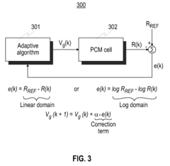
- Programming and verification methods: Advanced programming algorithms and verification techniques can be implemented to improve the operational uniformity of PCM devices. These methods include adaptive programming schemes, multi-pulse programming approaches, and real-time verification procedures. By dynamically adjusting programming parameters based on feedback from the memory cells, these techniques can compensate for inherent variations in device characteristics and ensure consistent performance.
- Material composition and interface engineering: The composition of phase change materials and the engineering of interfaces between different layers play crucial roles in determining device uniformity. By carefully selecting material compositions, controlling dopant concentrations, and optimizing interface properties, the variability in switching behavior can be minimized. Advanced materials with more stable phase transition characteristics can also contribute to improved uniformity across memory arrays.
- System-level approaches for managing non-uniformity: System-level solutions can be implemented to manage and compensate for inherent non-uniformities in PCM devices. These approaches include error correction codes, adaptive read schemes, and intelligent memory controllers. By incorporating these techniques, memory systems can maintain reliable operation despite variations in individual cell characteristics, effectively improving the perceived uniformity from a system perspective.
02 Cell structure designs for improved uniformity
Innovative cell structure designs can enhance the uniformity of phase change memory devices. These designs include optimized electrode configurations, specialized interface layers, and novel geometric arrangements of the phase change material. Such structural modifications help to ensure consistent current distribution and heat generation during programming operations, resulting in more uniform switching behavior across multiple memory cells.Expand Specific Solutions03 Programming and verification methods for uniform operation
Advanced programming and verification methods can be implemented to improve the operational uniformity of phase change memory devices. These methods include adaptive programming algorithms, multi-pulse programming schemes, and real-time verification techniques. By dynamically adjusting programming parameters based on cell-specific characteristics, these approaches can compensate for inherent variations in PCM cells and achieve more consistent resistance states.Expand Specific Solutions04 Material composition optimization for uniformity
The composition of phase change materials can be optimized to enhance device uniformity. This includes developing specialized chalcogenide alloys, incorporating dopants to stabilize material properties, and creating multi-layer phase change structures. These material innovations help to reduce variability in crystallization behavior, thermal characteristics, and resistance states, resulting in more uniform performance across PCM arrays.Expand Specific Solutions05 Memory architecture and control systems for uniform operation
System-level approaches to PCM uniformity involve specialized memory architectures and control systems. These include advanced addressing schemes, intelligent controller designs, and error correction mechanisms. By implementing sophisticated read/write protocols and compensation techniques at the system level, variations in individual PCM cells can be effectively managed to ensure uniform performance across the entire memory array.Expand Specific Solutions
Key Industry Players in PCM Development
The PCM device uniformity market is in a growth phase, characterized by increasing demand for reliable non-volatile memory solutions. The global market is expanding as Phase Change Memory technology matures, with projections showing significant growth potential. Leading semiconductor equipment manufacturers like Applied Materials, Lam Research, and Tokyo Electron are developing advanced process control solutions to address variability challenges. Meanwhile, memory manufacturers including Micron Technology, TSMC, and STMicroelectronics are investing in research to improve PCM device uniformity. Research institutions such as IMEC and Industrial Technology Research Institute collaborate with industry players to develop next-generation techniques. The competitive landscape features both established semiconductor giants and specialized equipment providers working to overcome the technical challenges of process variability in PCM manufacturing.
Taiwan Semiconductor Manufacturing Co., Ltd.
Technical Solution: TSMC has pioneered comprehensive process variability mitigation techniques for PCM device uniformity through their "Statistical Process Control Framework" specifically designed for phase change memory manufacturing. This framework incorporates advanced in-line metrology systems that continuously monitor critical dimensions and material properties throughout the fabrication process[1]. TSMC's approach includes proprietary deposition techniques that ensure uniform chalcogenide layer thickness and composition across 300mm wafers, addressing one of the primary sources of PCM variability. Their solution implements tight process control of the heater element dimensions through advanced lithography and etching techniques, maintaining consistent thermal profiles during programming operations[2]. TSMC has also developed specialized annealing processes that optimize the initial crystalline state of PCM materials, establishing a more uniform starting condition for all memory cells. Additionally, their manufacturing process incorporates advanced interface engineering between electrodes and phase change materials to minimize contact resistance variations[3].
Strengths: TSMC's manufacturing expertise and advanced process control capabilities enable industry-leading uniformity in PCM device characteristics. Their integrated approach addresses variability at multiple manufacturing stages rather than relying solely on circuit-level compensation. Weaknesses: The stringent process controls may result in higher manufacturing costs and potentially lower yields during initial production ramps. The approach may also be less adaptable to different PCM material systems without significant process modifications.
Micron Technology, Inc.
Technical Solution: Micron has developed advanced process variability mitigation techniques for PCM device uniformity through their innovative "Adaptive Write Algorithm" that dynamically adjusts programming parameters based on real-time feedback from individual cells. This approach compensates for manufacturing variations by applying customized programming pulses that account for cell-specific resistance distributions[1]. Their solution incorporates multi-level verification steps during the write process to ensure consistent resistance states across the memory array. Additionally, Micron has implemented specialized doping profiles and electrode materials that minimize the impact of process variations on SET/RESET operations[2]. Their technology includes thermal engineering solutions that control heat dissipation during programming, which is critical for maintaining uniform crystallization/amorphization processes across the PCM array. Micron has also developed advanced lithography techniques specifically optimized for PCM manufacturing to ensure consistent cell dimensions and material deposition[3].
Strengths: Micron's adaptive programming approach provides superior resilience against manufacturing variations while maintaining high performance. Their extensive experience in memory production enables practical, production-ready solutions. Weaknesses: The adaptive algorithms introduce additional complexity and potentially higher power consumption during write operations. The approach may also require more sophisticated control circuitry compared to simpler PCM implementations.
Critical Patents in PCM Uniformity Enhancement
Multilevel programming of phase change memory
PatentInactiveUS20110051508A1
Innovation
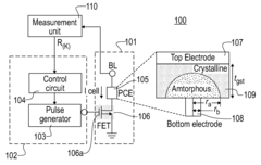
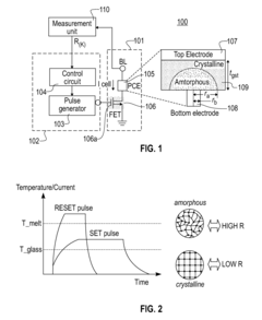
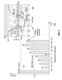
- A method involving a programming scheme that operates in two modes: annealing steps to approach a target resistance level and melting steps to adjust if the level is undershot, utilizing a pulse generator and control circuit to apply programming pulses efficiently, reducing the need for full-RESET pulses and minimizing power consumption.
Selective stop to control heater height variation
PatentPendingUS20230200270A1
Innovation
- A multi-step selective stop method is employed to control heater height variation by using a bi-layer dielectric and performing precise chemical mechanical planarization, removing excess heating material and sacrificial dielectric layers to achieve uniform heater heights across PCM cells.


Material Science Advancements for PCM Fabrication
The evolution of Phase Change Memory (PCM) technology has been significantly influenced by advancements in material science. Traditional PCM devices utilizing Ge2Sb2Te5 (GST) alloys have faced challenges related to process variability, which directly impacts device uniformity and reliability. Recent material science breakthroughs have focused on addressing these fundamental limitations through innovative approaches to PCM fabrication.
Doped chalcogenide materials have emerged as a promising solution to mitigate process variability. By incorporating dopants such as nitrogen, carbon, or silicon into GST alloys, researchers have demonstrated improved thermal stability and reduced atomic migration during cycling operations. These doped materials exhibit more consistent crystallization temperatures across devices, resulting in narrower resistance distribution and enhanced uniformity in large PCM arrays.
Interface engineering represents another critical advancement in PCM fabrication. The development of specialized buffer layers between the phase change material and electrodes has proven effective in controlling heat dissipation and reducing variability in the active switching volume. Materials such as TiN and TaN with precisely controlled thicknesses have been implemented to create more uniform thermal profiles during programming operations, thereby improving device-to-device consistency.
Atomic Layer Deposition (ALD) techniques have revolutionized PCM fabrication by enabling precise control over film thickness and composition at the atomic scale. This level of precision has been instrumental in reducing process variability, particularly for confined cell structures where material distribution uniformity is paramount. ALD-deposited PCM materials show significantly improved compositional homogeneity compared to traditional physical vapor deposition methods, resulting in more predictable switching behavior across devices.
Nanostructured phase change materials represent a cutting-edge approach to variability mitigation. By engineering PCM materials at the nanoscale through techniques such as superlattice structures or nanocomposites, researchers have achieved greater control over crystallization dynamics. These nanostructured materials demonstrate more deterministic phase transitions with reduced stochasticity, leading to tighter parameter distributions in fabricated devices.
Advanced annealing protocols have been developed to optimize the microstructure of deposited PCM films. Techniques such as rapid thermal annealing, laser annealing, and flash lamp annealing have been refined to promote uniform grain structure formation while minimizing elemental segregation. These controlled annealing processes significantly reduce the variability in initial resistance states and improve the consistency of switching behavior across manufactured devices.
Scaling Considerations for Next-Generation PCM Devices
As Phase Change Memory (PCM) technology advances toward higher densities and smaller feature sizes, several critical scaling considerations emerge that directly impact device uniformity and performance. The fundamental challenge lies in maintaining consistent switching behavior as cell dimensions shrink below 20nm. At these scales, the volume of phase change material becomes exceedingly small, leading to increased sensitivity to process variations and structural defects.
Thermal management becomes increasingly critical with scaling, as the thermal profile directly affects crystallization dynamics. Smaller cells experience faster heat dissipation due to increased surface-to-volume ratios, potentially altering the programming characteristics between devices. This thermal variability must be addressed through advanced materials engineering and novel cell architectures that provide better thermal confinement.
Material interface effects gain prominence at smaller dimensions, where the ratio of interface area to active material volume increases substantially. These interfaces can introduce nucleation sites that alter crystallization behavior unpredictably across devices. Research into interface engineering techniques, including the use of buffer layers and surface treatments, shows promise in mitigating these variations.
The scaling of electrode dimensions presents another significant challenge. As contact areas decrease, current density variations become more pronounced, leading to inconsistent Joule heating across the device array. Advanced electrode materials with improved conductivity uniformity and novel geometries that ensure consistent current distribution are being explored to address this issue.
Lithographic limitations also impact device uniformity at smaller nodes. Even minor variations in feature dimensions can translate to significant performance differences between cells. Multi-patterning techniques and extreme ultraviolet lithography offer improved precision but introduce their own process variations that must be carefully controlled.
Dopant distribution becomes increasingly difficult to control at smaller scales, yet remains crucial for tailoring crystallization properties. Statistical variations in dopant concentration can lead to device-to-device variability. Advanced deposition techniques with precise compositional control and post-deposition treatments are being developed to ensure uniform dopant profiles across large arrays.
Integration challenges with CMOS periphery circuits intensify with scaling, as the performance of selector devices must keep pace with the reduced dimensions of PCM cells. Co-optimization of memory cells and selectors is essential to maintain array uniformity while enabling high-density integration.
Unlock deeper insights with PatSnap Eureka Quick Research — get a full tech report to explore trends and direct your research. Try now!
Generate Your Research Report Instantly with AI Agent
Supercharge your innovation with PatSnap Eureka AI Agent Platform!