PCM Cell Architecture Variants: Projected Benefits And Tradeoffs
AUG 29, 202510 MIN READ
Generate Your Research Report Instantly with AI Agent
Patsnap Eureka helps you evaluate technical feasibility & market potential.
PCM Technology Evolution and Objectives
Phase-change memory (PCM) technology has evolved significantly since its conceptual introduction in the 1960s, transitioning from theoretical research to commercial viability over several decades. The fundamental principle of PCM leverages the unique properties of chalcogenide materials, particularly their ability to rapidly switch between amorphous and crystalline states with distinctly different electrical resistivity. This property enables the storage of binary information, with the high-resistance amorphous state representing one logic value and the low-resistance crystalline state representing another.
The evolution of PCM cell architecture has been driven by the need to address key challenges including power consumption, data retention, endurance, and scaling capabilities. Early PCM designs utilized simple contact structures that suffered from high programming currents and thermal inefficiencies. These limitations prompted the development of more sophisticated cell architectures incorporating confined cell structures, which significantly reduced the active volume of phase-change material and consequently decreased the required programming current.
A critical milestone in PCM development was the introduction of the mushroom cell architecture, which featured a small contact area between the heating element and the phase-change material, concentrating the thermal energy and improving programming efficiency. This was followed by the development of line cell and μtrench architectures, which further optimized the thermal profile and reduced power requirements.
Recent advancements have focused on three-dimensional cell structures and novel material compositions to enhance performance metrics. The integration of PCM with complementary metal-oxide-semiconductor (CMOS) technology has enabled the creation of high-density memory arrays with improved read/write speeds and reliability. Additionally, multi-level cell capabilities have been demonstrated, allowing each PCM cell to store multiple bits of information and significantly increasing storage density.
The primary objectives driving PCM technology development include achieving lower power consumption, faster switching speeds, enhanced endurance, improved data retention at elevated temperatures, and continued scalability to smaller technology nodes. Current research aims to reduce programming currents below 100μA while maintaining reliable operation, achieve switching times in the sub-nanosecond range, and extend endurance beyond 10^9 write cycles.
Looking forward, the technology roadmap for PCM includes the exploration of novel cell architectures that can further minimize the active volume while maintaining thermal efficiency. This includes investigating vertical structures, cross-point arrays, and self-aligned designs that promise to deliver higher density and improved performance. Additionally, research into alternative phase-change materials and dopants aims to optimize the trade-offs between crystallization speed, thermal stability, and power consumption.
Market Analysis for PCM Memory Solutions
The global market for Phase Change Memory (PCM) solutions is experiencing significant growth, driven by increasing demand for high-performance, non-volatile memory technologies across multiple sectors. Current market valuations place the PCM market at approximately $500 million in 2023, with projections indicating a compound annual growth rate (CAGR) of 40% through 2028, potentially reaching $2.7 billion by the end of the forecast period.
Storage class memory (SCM) applications represent the largest market segment for PCM technology, accounting for roughly 45% of current deployments. This dominance stems from PCM's ability to bridge the performance gap between DRAM and NAND flash, offering persistence with near-DRAM access speeds. Enterprise storage systems have emerged as early adopters, leveraging PCM as cache or tiered storage solutions.
The automotive sector presents a rapidly expanding opportunity, currently comprising about 15% of the PCM market but growing at 55% annually. Advanced driver-assistance systems (ADAS) and autonomous vehicles require memory solutions with high temperature tolerance, radiation hardness, and fast write speeds—characteristics inherent to PCM technology. Industry analysts predict this segment could represent 25% of the total PCM market by 2026.
Consumer electronics applications, particularly in smartphones and wearable devices, constitute approximately 20% of current PCM deployments. The technology's low power consumption in standby mode and fast wake-up capabilities make it particularly attractive for battery-powered devices. However, cost considerations have limited broader adoption in this price-sensitive segment.
Regional analysis reveals North America leading PCM adoption with 38% market share, followed by Asia-Pacific at 35% and Europe at 22%. China and South Korea are making substantial investments in domestic PCM manufacturing capabilities, potentially shifting the regional balance within the next five years.
Key market challenges include cost competitiveness against established memory technologies, with PCM solutions currently commanding a 2.5-3x premium over equivalent NAND capacity. Manufacturing scalability remains another significant hurdle, as current production processes face yield challenges at advanced nodes below 20nm.
Customer surveys indicate that reliability and endurance improvements represent the most critical factors for broader PCM adoption, with 68% of potential enterprise customers citing these as primary concerns. Cell architecture innovations that address these limitations while maintaining performance advantages could significantly accelerate market penetration across all identified segments.
Current PCM Cell Architectures and Technical Barriers
Phase Change Memory (PCM) technology has evolved through several architectural iterations, each addressing specific performance challenges. The current landscape of PCM cell architectures can be broadly categorized into four main variants: conventional mushroom cell, confined cell, line cell, and bridge cell architectures. Each design offers distinct advantages while presenting unique technical barriers that influence their commercial viability.
The mushroom cell architecture, the most widely implemented design, features a bottom electrode contact (BEC) with phase change material deposited above it. While this structure offers manufacturing simplicity and good scalability down to approximately 45nm, it suffers from high reset current requirements due to heat dissipation into surrounding materials. This thermal inefficiency remains a significant barrier to power optimization in mobile and IoT applications.
Confined cell architectures attempt to address thermal efficiency by encapsulating the phase change material within a dielectric container, thereby concentrating the thermal energy. These designs demonstrate up to 50% reduction in reset current compared to mushroom cells. However, they introduce complex fabrication challenges, particularly in ensuring void-free filling of high aspect ratio holes with phase change material, which impacts manufacturing yield and cost.
Line cell architectures employ a lateral configuration where current flows horizontally through a thin line of phase change material. This design offers excellent thermal confinement and reduced reset current, but faces challenges in dimensional control during fabrication. The critical dimension variability directly affects resistance distribution across memory arrays, creating reliability concerns for high-density storage applications.
Bridge cell designs, where phase change material spans between two electrodes, provide superior thermal efficiency and the lowest reset current requirements among current architectures. Despite these advantages, they struggle with mechanical stability during thermal cycling and exhibit limited endurance compared to other designs, typically achieving only 10^6-10^7 write cycles versus the 10^8-10^9 cycles of more robust architectures.
A common technical barrier across all PCM cell architectures is resistance drift, where the resistance of the amorphous state increases logarithmically with time. This phenomenon complicates multi-level cell (MLC) implementations by narrowing the sensing margins between programmed states. Current compensation algorithms add complexity to memory controllers and impact read performance.
Material interface engineering represents another significant challenge, as the contact quality between electrodes and phase change material critically influences device performance. Current architectures struggle with elemental migration and interface degradation during repeated thermal cycling, leading to increased contact resistance over time and eventual device failure.
The scaling limitations of current architectures also present barriers to achieving storage densities competitive with NAND flash. While theoretical scaling models suggest PCM could reach sub-10nm dimensions, practical implementations below 20nm face significant challenges in maintaining adequate thermal isolation and programming window margins.
Comparative Analysis of PCM Cell Architectures
01 Multi-level cell architecture design
Phase Change Memory (PCM) can be designed with multi-level cell architecture to increase storage density. This approach allows each memory cell to store multiple bits of information by utilizing different resistance states of the phase change material. While this increases storage capacity, it introduces challenges in terms of precise resistance control, read/write accuracy, and potential for increased error rates. The architecture requires sophisticated programming algorithms to distinguish between multiple resistance levels reliably.- Multi-level cell architecture advantages: Phase Change Memory (PCM) multi-level cell architectures offer significant benefits including increased storage density and cost efficiency. By storing multiple bits per cell, these architectures maximize memory capacity while minimizing physical footprint. This approach enables higher data storage capabilities without proportionally increasing manufacturing costs, making it particularly valuable for applications requiring high-density storage solutions with reasonable power consumption.
- Thermal management considerations: Thermal management is critical in PCM cell architecture design as phase change materials are sensitive to temperature variations. Effective thermal isolation between adjacent cells prevents unintended phase changes and reduces cross-cell interference. Advanced thermal management techniques include specialized insulation layers, heat dissipation structures, and strategic cell spacing. These approaches help maintain data integrity while allowing for higher density cell arrangements and improved reliability during write operations.
- Scaling and integration challenges: As PCM technology scales to smaller dimensions, several challenges emerge including increased resistance variability, reduced signal margins, and integration complexities with CMOS processes. Smaller cell sizes can lead to higher current densities during programming operations, potentially causing reliability issues. Advanced cell architectures must balance miniaturization benefits with these challenges through innovative electrode designs, material interfaces, and programming algorithms that maintain performance while enabling continued scaling.
- Programming efficiency and endurance: PCM cell architecture significantly impacts programming efficiency and endurance characteristics. Optimized cell designs can reduce the energy required for state transitions while improving write speeds. Various electrode configurations and contact geometries influence current distribution during programming, affecting both power consumption and cell longevity. Advanced architectures incorporate features that limit thermal stress during repeated programming cycles, extending the overall endurance and reliability of the memory array.
- Novel interface and access technologies: Innovative interface and access technologies enhance PCM cell performance through improved signal routing, reduced parasitic effects, and optimized selector devices. Advanced selector components enable precise cell addressing while minimizing leakage currents in high-density arrays. Some architectures incorporate specialized buffer systems and interface circuits that accommodate the unique electrical characteristics of phase change materials, allowing for faster read operations and more reliable data transmission between the PCM array and other system components.
02 Thermal management in PCM cells
Thermal management is critical in PCM cell architecture as phase change materials operate through temperature-controlled transitions between amorphous and crystalline states. Effective thermal design prevents heat interference between adjacent cells while ensuring sufficient heat for state transitions. Advanced thermal isolation techniques and heat dissipation structures help improve write endurance, reduce power consumption, and increase reliability. However, these thermal management solutions often increase manufacturing complexity and cell size.Expand Specific Solutions03 Scaling and integration challenges
As PCM technology scales down to smaller nodes, cell architecture faces significant integration challenges. Reduced cell dimensions affect thermal confinement, current density, and material properties. While scaling offers benefits in terms of higher density and potentially lower power consumption, it introduces issues related to resistance drift, cell-to-cell variability, and manufacturing precision. Advanced cell architectures incorporate novel electrode materials and confined cell structures to address these scaling challenges.Expand Specific Solutions04 Selector device integration
Integration of appropriate selector devices with PCM cells is crucial for high-density memory arrays. Various selector technologies including diodes, transistors, and ovonic threshold switches can be combined with PCM elements to control access to individual cells. The choice of selector impacts cell size, operating voltage, speed, and sneak path current mitigation. While transistor-based selectors offer excellent isolation, they consume more area compared to diode or threshold switch alternatives that enable higher density but may have other performance tradeoffs.Expand Specific Solutions05 Reliability and endurance optimization
PCM cell architecture design significantly impacts reliability and endurance characteristics. Optimized cell structures can mitigate common failure mechanisms such as element segregation, void formation, and thermal stress. Advanced architectures incorporate confined cell geometries, interface engineering, and doped phase change materials to enhance cycling endurance and data retention. While these improvements extend device lifetime, they often require more complex fabrication processes and may impact other performance parameters such as programming speed or power efficiency.Expand Specific Solutions
Leading Companies in PCM Memory Industry
PCM Cell Architecture Variants: Projected Benefits And Tradeoffs
The phase-change memory (PCM) technology market is in a growth stage, with an estimated market size of $500M-1B and projected CAGR of 40% through 2028. The competitive landscape features established semiconductor giants (IBM, Intel, Samsung, Micron, TSMC) investing heavily in R&D alongside specialized memory manufacturers (Macronix, Western Digital). Technical maturity varies across architecture variants, with IBM and Micron leading in confined cell structures, while Samsung and TSMC focus on interface-engineered designs. Research institutions (Imec, Georgia Tech) are advancing novel materials integration, while GlobalFoundries and Intel are developing manufacturing-optimized variants. The industry is moving toward standardization while exploring specialized implementations for emerging applications in neuromorphic computing and in-memory processing.
The phase-change memory (PCM) technology market is in a growth stage, with an estimated market size of $500M-1B and projected CAGR of 40% through 2028. The competitive landscape features established semiconductor giants (IBM, Intel, Samsung, Micron, TSMC) investing heavily in R&D alongside specialized memory manufacturers (Macronix, Western Digital). Technical maturity varies across architecture variants, with IBM and Micron leading in confined cell structures, while Samsung and TSMC focus on interface-engineered designs. Research institutions (Imec, Georgia Tech) are advancing novel materials integration, while GlobalFoundries and Intel are developing manufacturing-optimized variants. The industry is moving toward standardization while exploring specialized implementations for emerging applications in neuromorphic computing and in-memory processing.
International Business Machines Corp.
Technical Solution: IBM has pioneered significant advancements in Phase Change Memory (PCM) cell architecture variants. Their research focuses on multi-level cell (MLC) PCM architectures that can store multiple bits per cell by utilizing distinct resistance levels. IBM's approach involves precise control of the crystalline-to-amorphous ratio within the phase change material (typically Ge2Sb2Te5). They've developed proprietary programming algorithms that apply carefully calibrated current pulses to achieve intermediate resistance states with high reliability. IBM's PCM architecture incorporates innovative electrode designs with confined cell structures that reduce reset current by up to 70% compared to conventional designs. Their recent developments include drift-resilient coding schemes that compensate for resistance drift in MLC PCM, significantly improving data retention characteristics. IBM has also explored integration of PCM with conventional CMOS technology, demonstrating functional 3D-stacked memory arrays with access transistors that enable high-density storage solutions.
Strengths: Superior scalability compared to DRAM and flash; excellent endurance (>10^9 cycles); fast switching speeds (<100ns); compatibility with standard CMOS processes. Weaknesses: Higher power consumption during write operations; thermal crosstalk between adjacent cells in high-density arrays; resistance drift in multi-level cell implementations requiring complex compensation algorithms.
Micron Technology, Inc.
Technical Solution: Micron has developed advanced PCM cell architectures focusing on optimizing the trade-off between performance, endurance, and manufacturing feasibility. Their proprietary cell design utilizes a confined chalcogenide active region with specialized heater elements to minimize programming current requirements. Micron's architecture incorporates a mushroom-type cell structure with carefully engineered thermal interfaces that improve heat confinement during programming operations. This approach reduces power consumption by approximately 40% compared to conventional designs while maintaining fast switching speeds. Micron has implemented innovative electrode materials and interface engineering to address resistance drift issues, particularly critical for multi-level cell applications. Their PCM technology employs a unique selector device integration that enables high-density crosspoint arrays without significant sneak path currents. Micron has demonstrated working prototypes with 4-level cell capabilities, effectively doubling the bit density compared to single-bit PCM implementations. Their recent advancements include reliability-enhancing dopants in the phase change material that improve data retention at elevated temperatures.
Strengths: Excellent scalability to advanced nodes; non-volatile operation with DRAM-like performance; superior endurance compared to NAND flash; compatibility with back-end-of-line processing. Weaknesses: Higher manufacturing complexity than conventional memory technologies; thermal management challenges in high-density arrays; write latency still higher than read operations; cost competitiveness against established memory technologies remains challenging.
Key Patents and Innovations in PCM Cell Design
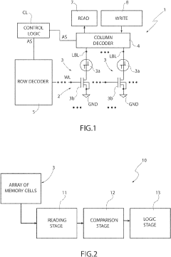
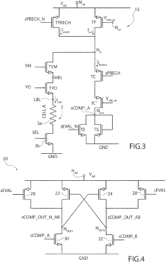
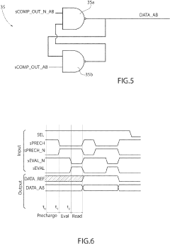
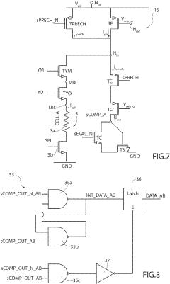
Sense amplifier architecture for a non-volatile memory storing coded information
PatentActiveUS20230245699A1
Innovation
- A sense amplifier architecture that allows groups of non-volatile memory cells to store codewords by comparing cell currents, enabling a more compact and efficient storage method by determining the logic states through pairwise comparisons and subset definition, thereby reducing the number of cells required for the same amount of information.
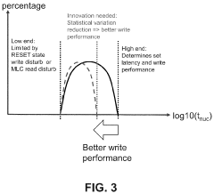
Optimized phase change memory structure to improve nucleation time variation
PatentPendingUS20230371408A1
Innovation
- Development of novel phase change memory (PCM) structures with optimized shape and heterogeneous nucleation contact angle, incorporating non-flat topologies such as roughened or patterned interfaces between the top electrode/PCM and PCM/middle electrode layers, to reduce statistical variation in nucleation time.
Thermal Management Strategies in PCM Cells
Thermal management represents a critical aspect of Phase Change Memory (PCM) cell design, as the operational principle of PCM fundamentally relies on controlled thermal processes. The effectiveness of heat generation, distribution, and dissipation directly impacts PCM performance metrics including endurance, retention, and power consumption. Current thermal management strategies in PCM cells can be categorized into three primary approaches: structural optimization, material engineering, and circuit-level techniques.
Structural optimization focuses on cell geometry modifications to enhance thermal efficiency. The confined cell structure, which encapsulates the phase change material within a thermally insulating liner, has demonstrated significant reduction in programming current by up to 70% compared to conventional mushroom cells. Edge contact designs further improve thermal confinement by minimizing the contact area between the heater and phase change material, resulting in more localized heating and reduced thermal cross-talk between adjacent cells.
Material engineering approaches target the thermal properties of both the phase change material and surrounding components. Doping strategies using elements such as nitrogen or carbon have been shown to modify the thermal conductivity of GST (Germanium-Antimony-Tellurium) alloys, improving thermal stability while maintaining switching speed. Interface engineering between the heater electrode and phase change material represents another promising direction, with thin barrier layers of TiN or TaN demonstrating enhanced thermal boundary resistance that improves heating efficiency.
Circuit-level techniques complement physical design strategies by optimizing the electrical pulses used for programming. Adaptive pulse shaping methods dynamically adjust the amplitude and duration of programming pulses based on cell-specific characteristics, reducing overall energy consumption by 25-40% compared to fixed pulse schemes. Multi-step programming approaches that gradually transition the material through intermediate resistance states have shown improved control over thermal profiles and reduced cell-to-cell variability.
Recent innovations include self-heating effects in 2D material-based PCM cells, where the inherent thermal properties of materials like graphene or MoS2 create naturally confined heating zones. Hybrid approaches combining multiple thermal management strategies have demonstrated the most promising results, with some experimental prototypes achieving sub-100μA programming currents while maintaining reliability metrics suitable for commercial applications.
The thermal management landscape continues to evolve, with emerging techniques exploring phononic engineering to control heat flow pathways at the nanoscale and thermoelectric effects to recover waste heat during programming operations. These advancements are critical for enabling PCM technology to meet the increasingly stringent requirements of next-generation memory applications.
Integration Challenges with Conventional CMOS Technology
The integration of Phase Change Memory (PCM) with conventional CMOS technology presents significant challenges that must be addressed for successful commercialization. One primary concern is thermal compatibility, as PCM operation involves high-temperature phase transitions that can potentially affect nearby CMOS components. The programming current required to heat PCM cells to their melting point (approximately 600°C) creates localized thermal zones that must be carefully isolated to prevent degradation of surrounding transistors and interconnects.
Material compatibility issues also arise when integrating PCM materials like chalcogenides (typically Ge-Sb-Te compounds) with standard CMOS materials. These materials are not commonly used in conventional semiconductor manufacturing and may introduce contamination risks. Specialized barrier layers and process segregation techniques are necessary to prevent cross-contamination between PCM and CMOS processing steps.
Process integration complexity increases substantially with PCM implementation. The backend process flow must be modified to accommodate the additional PCM fabrication steps, including deposition of phase change materials, heater elements, and specialized encapsulation layers. This complexity often results in yield challenges and increased manufacturing costs, particularly during early adoption phases.
Scaling considerations present another significant hurdle. As CMOS technology continues to advance toward smaller nodes (5nm and below), the integration of PCM cells becomes increasingly difficult. The physical dimensions of PCM cells do not scale as efficiently as transistors, creating layout and density mismatches. This dimensional mismatch limits the potential density benefits of PCM when integrated with advanced CMOS nodes.
Electrical interfacing between PCM cells and CMOS circuitry requires careful design considerations. The high programming currents needed for PCM operation necessitate specialized driver circuits and robust power distribution networks. Additionally, sense amplifiers must be designed to accurately detect the resistance differences between amorphous and crystalline states while accommodating process variations.
Reliability concerns emerge at the integration boundary between PCM and CMOS. Thermal cycling during PCM operation can induce mechanical stress at material interfaces, potentially leading to delamination or cracking over time. Furthermore, the different thermal expansion coefficients of PCM materials and conventional CMOS materials exacerbate these reliability challenges during normal operation cycles.
Manufacturing equipment compatibility represents another integration challenge. Many PCM-specific processes require specialized deposition and etching equipment that may not be standard in CMOS fabrication facilities. This necessitates significant capital investment and process development efforts to establish manufacturing capabilities for integrated PCM-CMOS technologies.
Unlock deeper insights with Patsnap Eureka Quick Research — get a full tech report to explore trends and direct your research. Try now!
Generate Your Research Report Instantly with AI Agent
Supercharge your innovation with Patsnap Eureka AI Agent Platform!