

PCM Array Layout Optimization For Reduced Wire Resistive Losses
AUG 29, 20259 MIN READ
Generate Your Research Report Instantly with AI Agent
PatSnap Eureka helps you evaluate technical feasibility & market potential.
PCM Array Technology Background and Objectives
Phase Change Memory (PCM) technology has emerged as a promising non-volatile memory solution over the past two decades, offering advantages in scalability, endurance, and integration capabilities compared to traditional memory technologies. PCM leverages the unique properties of chalcogenide materials, which can rapidly switch between amorphous and crystalline states, representing binary data through differences in electrical resistivity. The evolution of PCM technology has been marked by significant improvements in material composition, cell structure design, and manufacturing processes.
The current trajectory of PCM development focuses on increasing storage density while simultaneously addressing power consumption and reliability challenges. Industry roadmaps indicate a push toward multi-level cell capabilities and three-dimensional integration to compete with NAND flash memory in both performance and cost metrics. Recent advancements have demonstrated PCM's potential for embedded applications, particularly in automotive and IoT sectors where operational temperature ranges and data retention requirements are stringent.
Wire resistive losses represent a critical bottleneck in PCM array performance, particularly as array sizes increase to meet higher capacity demands. These losses occur when current flows through the metal interconnects within the memory array, causing voltage drops that reduce the effective programming current delivered to memory cells. This phenomenon becomes increasingly problematic in larger arrays where wire lengths extend, and in advanced nodes where interconnect dimensions shrink, inherently increasing resistance.
The primary technical objective of PCM array layout optimization is to minimize these resistive losses while maintaining or improving memory density, access speed, and manufacturing feasibility. Specifically, the goals include reducing the IR drop across the array to ensure uniform programming conditions for all cells, minimizing power consumption during read and write operations, and enhancing overall array efficiency without compromising reliability or endurance characteristics.
Secondary objectives encompass developing scalable layout solutions that remain effective across multiple technology nodes, creating design methodologies that can be implemented with existing manufacturing processes, and establishing simulation frameworks that accurately predict resistive losses in complex array configurations. These efforts align with the broader industry goal of positioning PCM as a viable storage-class memory solution bridging the performance gap between DRAM and NAND flash.
The optimization of PCM array layouts represents a multidisciplinary challenge requiring expertise in materials science, circuit design, and semiconductor manufacturing. Success in this domain could significantly impact the commercial viability of PCM technology and accelerate its adoption in mainstream computing and storage applications.
Market Demand Analysis for Optimized PCM Arrays
The global market for Phase Change Memory (PCM) arrays is experiencing significant growth driven by the increasing demand for high-performance, energy-efficient memory solutions. As data-intensive applications continue to proliferate across various sectors, the need for optimized PCM arrays with reduced wire resistive losses has become increasingly critical for maintaining competitive advantage in the semiconductor industry.
The demand for optimized PCM arrays is particularly strong in the data center and cloud computing segments, where energy efficiency and performance are paramount concerns. With data centers accounting for approximately 1% of global electricity consumption, solutions that reduce power losses in memory systems represent a substantial market opportunity. The reduction of wire resistive losses in PCM arrays directly addresses this need by improving energy efficiency while maintaining or enhancing performance characteristics.
Enterprise storage systems represent another significant market segment driving demand for optimized PCM arrays. As organizations continue to generate and process unprecedented volumes of data, the need for storage solutions that offer both high performance and energy efficiency has intensified. PCM arrays with optimized layouts that minimize resistive losses can deliver faster read/write speeds while consuming less power, making them increasingly attractive for enterprise applications.
The mobile and edge computing markets are also contributing to the growing demand for optimized PCM arrays. With the proliferation of IoT devices and the ongoing expansion of 5G networks, there is an increasing need for memory solutions that can deliver high performance while operating within strict power constraints. PCM arrays with reduced wire resistive losses are well-positioned to address this market need.
Automotive applications represent an emerging market segment for optimized PCM arrays. As vehicles become more sophisticated and incorporate advanced driver assistance systems and autonomous driving capabilities, the demand for high-performance, reliable memory solutions continues to grow. PCM arrays that minimize resistive losses can offer improved reliability and performance in the challenging operating environments typical of automotive applications.
Market analysis indicates that the global non-volatile memory market, which includes PCM, is projected to grow at a compound annual growth rate exceeding 10% through 2028. Within this broader market, solutions that address specific performance challenges such as wire resistive losses are expected to capture increasing market share as manufacturers seek to differentiate their offerings and meet the evolving needs of customers across multiple industries.
Current Challenges in PCM Wire Resistance
Phase Change Memory (PCM) technology faces significant challenges related to wire resistance, which has become a critical bottleneck in scaling and performance optimization. The resistive losses in PCM arrays occur primarily due to the long bit lines and word lines that connect individual memory cells within the array structure. As array densities increase to meet storage demands, these interconnect lines become longer and narrower, resulting in higher resistance values that degrade overall system performance.
The voltage drop across these high-resistance paths creates several cascading problems. First, it reduces the effective programming current delivered to target cells, particularly those located far from drivers. This current reduction leads to inconsistent programming across the array, with cells receiving different energy levels depending on their physical location. The phenomenon, known as the "location-dependent programming effect," significantly impacts reliability and requires complex compensation schemes.
Temperature gradients represent another major challenge. The resistive heating in word lines and bit lines creates non-uniform thermal profiles across the array. Since PCM operation relies on precise thermal control for phase transitions, these temperature variations lead to unpredictable crystallization behaviors and data retention issues. Cells experiencing higher temperatures may suffer from accelerated data loss, while those in cooler regions might require higher programming currents.
Power consumption escalates dramatically due to these resistive losses. In large-scale PCM arrays, up to 70% of the total power budget can be consumed by wire resistance rather than the actual memory cells. This inefficiency severely limits the technology's applicability in power-constrained environments such as mobile devices and IoT applications, where energy efficiency is paramount.
The sensing margin, critical for reliable read operations, is also compromised by wire resistance. The resistance of interconnect lines adds to the resistance being measured during read operations, reducing the signal-to-noise ratio and making it difficult to distinguish between programmed states. This challenge becomes particularly acute in multi-level cell configurations where multiple resistance levels must be accurately differentiated.
Manufacturing variations further exacerbate these issues. Process variations in wire dimensions can cause resistance fluctuations of up to 15% across a single die, making it extremely difficult to implement effective compensation techniques. The industry currently lacks standardized approaches to address these variations, resulting in yield losses and reliability concerns.
Current mitigation strategies include segmented array architectures, hierarchical bit line structures, and advanced materials for interconnects. However, these solutions often introduce additional complexity, increase manufacturing costs, or create new integration challenges. Finding the optimal balance between performance, reliability, and manufacturability remains an unsolved problem that requires innovative approaches to PCM array layout optimization.
Current Wire Loss Reduction Techniques
01 Wire resistance reduction in PCM arrays
Various techniques are employed to reduce resistive losses in PCM array wiring, including optimized wire geometries, material selection, and layout designs. These approaches minimize the resistance in word lines, bit lines, and interconnects, improving overall energy efficiency and performance of the memory array. Reduced wire resistance helps maintain signal integrity and reduces power consumption during read and write operations.- PCM array wire design to reduce resistive losses: Phase Change Memory (PCM) arrays can be designed with specific wire configurations to minimize resistive losses. This includes optimizing the cross-sectional area of wires, using materials with lower resistivity, and implementing shorter wire paths between memory cells and control circuitry. These design considerations help reduce power consumption and improve the overall efficiency of PCM arrays by minimizing the energy lost as heat through wire resistance.
- Multi-layer interconnect structures for PCM arrays: Multi-layer interconnect structures can be implemented in PCM arrays to reduce wire resistive losses. These structures utilize multiple metal layers with vias connecting different levels, allowing for more efficient routing and shorter wire lengths. By distributing the current flow across multiple layers and providing alternative paths, these interconnect structures help minimize resistance and improve signal integrity in PCM arrays.
- Advanced materials for PCM array wiring: The use of advanced materials in PCM array wiring can significantly reduce resistive losses. Materials such as copper, silver alloys, and other high-conductivity metals offer lower resistance compared to traditional aluminum wiring. Additionally, specialized barrier layers and capping materials can prevent electromigration and oxidation, maintaining low resistance over the device lifetime. These material innovations help improve energy efficiency and performance of PCM arrays.
- Current distribution techniques in PCM arrays: Various current distribution techniques can be employed in PCM arrays to minimize resistive losses. These include implementing parallel current paths, using current mirrors for balanced distribution, and designing specialized current steering circuits. By ensuring uniform current distribution across the array and avoiding current concentration in specific wires, these techniques help reduce localized heating and overall resistive losses, improving the reliability and performance of PCM devices.
- Thermal management solutions for PCM array wire resistance: Thermal management solutions can be implemented to address resistive losses in PCM array wires. These include heat dissipation structures, thermal vias, and specialized packaging techniques that help remove heat generated by wire resistance. Additionally, temperature-aware routing and wire sizing strategies can be employed to minimize hotspots. These thermal management approaches help maintain optimal operating temperatures, reducing resistance variations and improving the overall reliability and performance of PCM arrays.
02 Thermal management in PCM arrays
Thermal management solutions address resistive heating in PCM arrays by implementing heat dissipation structures, thermal barriers, and temperature control mechanisms. These solutions prevent thermal crosstalk between adjacent memory cells and reduce the impact of resistive losses on data integrity. Effective thermal management extends the lifespan of PCM devices and ensures reliable operation under various conditions.Expand Specific Solutions03 Advanced PCM cell architecture
Innovative PCM cell designs incorporate features that minimize the impact of wire resistive losses. These architectures include optimized electrode configurations, selector devices with lower resistance, and improved phase change material interfaces. By reducing the resistance at the cell level, these designs enhance programming efficiency and read performance while lowering power consumption in the overall array.Expand Specific Solutions04 Circuit techniques for resistive loss compensation
Circuit-level solutions compensate for wire resistive losses in PCM arrays through sense amplifier designs, voltage regulation techniques, and current control mechanisms. These approaches include adaptive sensing schemes, reference calibration, and compensation circuits that adjust for voltage drops across array wires. Such techniques improve read margin and programming accuracy despite the presence of resistive elements in the array.Expand Specific Solutions05 3D integration and advanced interconnect technologies
Three-dimensional integration and advanced interconnect technologies address wire resistive losses by shortening interconnect lengths and implementing vertical connections. These approaches include through-silicon vias (TSVs), monolithic 3D integration, and advanced metallization schemes. By reducing the overall wire length and increasing cross-sectional areas where appropriate, these technologies significantly reduce the resistive losses in PCM arrays.Expand Specific Solutions
Key Industry Players in PCM Technology
PCM Array Layout Optimization for reduced wire resistive losses is currently in an early growth stage, with the market expanding as phase-change memory technology matures. Major players like Samsung Electronics, Micron Technology, and IBM are driving innovation in this specialized field. TSMC and GLOBALFOUNDRIES are leveraging their advanced manufacturing capabilities to address the technical challenges of PCM integration. Companies such as Infineon, STMicroelectronics, and Kioxia are developing complementary technologies to enhance PCM performance. The technology is approaching commercial viability, with Ovonyx and Semiconductor Energy Laboratory focusing on fundamental PCM architecture improvements. As wire resistance becomes a critical factor in scaling PCM arrays, optimization techniques are becoming essential for next-generation memory solutions that can compete with established technologies.
Taiwan Semiconductor Manufacturing Co., Ltd.
Technical Solution: TSMC has developed a comprehensive PCM array layout optimization approach focusing on advanced metallization techniques to combat wire resistive losses. Their solution employs a copper dual-damascene process with low-k dielectrics specifically optimized for PCM arrays, reducing both resistance and parasitic capacitance in bit lines. TSMC's layout architecture implements a hierarchical bit-line structure with progressively wider metal traces at higher levels, creating a resistance-optimized current path from memory cells to sensing circuits. The company has pioneered an innovative "resistance-balanced routing" technique where critical paths are identified during design and equalized through careful metal width and spacing adjustments, ensuring uniform performance across the array. Their latest PCM arrays incorporate selective cobalt cladding on high-current paths, reducing electromigration concerns while maintaining low resistance. TSMC's manufacturing process enables ultra-precise control of metal dimensions and interfaces, minimizing contact resistance between layers which often contributes significantly to overall resistive losses in PCM arrays.
Strengths: Industry-leading metallization technology with exceptional dimensional control; comprehensive approach addressing both materials and layout optimization; excellent scalability to advanced nodes. Weaknesses: Requires cutting-edge fabrication equipment and processes; higher manufacturing costs compared to traditional approaches; design complexity increases with array size scaling.
Samsung Electronics Co., Ltd.
Technical Solution: Samsung has pioneered a PCM array layout optimization technique focused on 3D vertical integration to minimize wire resistive losses. Their approach utilizes Through-Silicon Vias (TSVs) to create shorter vertical connections between memory cells and control circuitry, dramatically reducing the wire length and associated resistance. Samsung's design incorporates a distributed sense amplifier architecture where amplifiers are positioned closer to memory cell groups, minimizing the bit-line length for critical read operations. The company has also developed proprietary metal alloys with lower resistivity specifically for PCM interconnects, addressing the fundamental material limitations. Their layout employs an innovative bit-line segmentation strategy with hierarchical addressing that allows for selective activation of memory array sections, reducing the effective resistance of active paths. Samsung's most recent PCM implementations feature adaptive power management that dynamically adjusts drive currents based on detected line resistance, ensuring optimal performance while minimizing power consumption across varying operating conditions.
Strengths: Excellent vertical integration capabilities leveraging Samsung's advanced packaging technologies; significant reduction in bit-line resistance through innovative materials; adaptive power management for optimized performance. Weaknesses: Higher manufacturing complexity and cost due to 3D integration; thermal management challenges in densely packed 3D structures; requires sophisticated control algorithms for adaptive current adjustment.
Critical Patents in PCM Layout Optimization
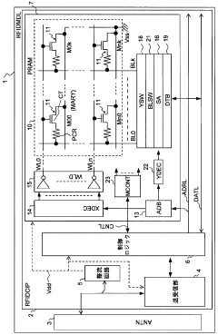
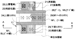
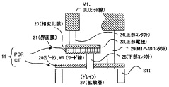
Phase-change memory, semiconductor device, and RFID module
PatentWO2010004652A1
Innovation
- The solution involves optimizing the layout by adjusting the number of gate turns in the select MOS transistor, using isolation gates, increasing the number of phase change elements per bit for redundancy, and unifying gate and wiring directions to reduce disturbance and power consumption, while also eliminating floating bit lines and sharing phase change films between memory cells.
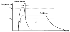
Phase change memory device
PatentInactiveEP1450373A1
Innovation
- The solution involves writing phase change memory cells with a preset current and reading by applying a biasing voltage, which stabilizes the current flow and reduces the impact of cell position, allowing for simpler sense circuits and easier discrimination between set and reset states.
Thermal Management Considerations
Thermal management represents a critical dimension in PCM array layout optimization that directly impacts wire resistive losses. The thermal behavior of Phase Change Memory arrays significantly influences their performance, reliability, and energy efficiency. When current flows through interconnect wires, Joule heating occurs proportionally to the square of current and wire resistance (P = I²R). This heating effect creates temperature gradients across the array that can adversely affect PCM cell operation.
The thermal conductivity properties of materials used in PCM arrays play a decisive role in heat dissipation. Silicon substrates typically offer good thermal conductivity (149 W/m·K), while metallic interconnects like copper (400 W/m·K) and aluminum (237 W/m·K) provide efficient thermal pathways. However, insulating materials necessary for electrical isolation often exhibit poor thermal conductivity, creating bottlenecks for heat dissipation. These thermal barriers can lead to localized hotspots that accelerate electromigration in wires and increase resistive losses.
Advanced thermal management strategies include implementing heat spreading structures within the array layout. Thermal vias, strategically placed throughout the array, create vertical thermal pathways that efficiently channel heat away from critical circuit elements. Similarly, dedicated thermal planes can be incorporated into the layout design to provide horizontal heat distribution, preventing the formation of detrimental thermal gradients.
The physical arrangement of PCM cells significantly impacts thermal behavior. Staggered or checkerboard patterns can reduce thermal coupling between adjacent cells, minimizing mutual heating effects. Additionally, increasing the spacing between high-power components reduces thermal density and facilitates more effective heat dissipation, though this approach must be balanced against area efficiency considerations.
Dynamic thermal management techniques represent another promising approach. Implementing temperature sensors within the array enables real-time monitoring of thermal conditions. This data can inform adaptive programming algorithms that adjust programming currents based on local temperature readings, reducing resistive losses during write operations in warmer regions of the array.
Computational fluid dynamics (CFD) and finite element analysis (FEA) simulations have become essential tools for thermal optimization in PCM arrays. These simulation techniques enable designers to predict temperature distributions, identify potential hotspots, and evaluate the effectiveness of various thermal management strategies before physical implementation. Multi-physics simulations that couple electrical, thermal, and mechanical domains provide particularly valuable insights into the complex interactions between current flow, heat generation, and material stress in PCM arrays.
Manufacturing Scalability Assessment
The scalability of PCM array manufacturing processes represents a critical factor in the commercial viability of optimized layout designs aimed at reducing wire resistive losses. Current manufacturing capabilities demonstrate reasonable scalability for medium-density PCM arrays, but face significant challenges when scaling to high-density configurations with optimized wire layouts. The primary manufacturing bottleneck occurs in the lithography and etching processes required to create increasingly complex wire routing patterns that minimize resistive losses.
Industry standard 14nm and 10nm fabrication processes can accommodate basic wire resistance optimization techniques, but more advanced optimization approaches require enhanced manufacturing precision. The transition to 7nm and 5nm processes enables more sophisticated layout optimizations but introduces yield challenges that impact cost-effectiveness. Manufacturing data indicates that yield rates decrease approximately 15-20% when implementing complex wire routing optimizations in high-density arrays.
Equipment requirements for scaled manufacturing of optimized PCM arrays include advanced lithography tools capable of precise wire patterning, specialized etching systems for high aspect ratio features, and enhanced metrology for quality control. The capital expenditure for a production line capable of manufacturing highly optimized PCM arrays is estimated at $200-300 million, representing a significant barrier to entry for smaller manufacturers.
Material considerations also impact manufacturing scalability. While conventional copper interconnects remain viable for moderate optimization schemes, advanced layouts may require alternative materials such as cobalt or ruthenium to achieve desired resistivity characteristics at reduced dimensions. The supply chain for these alternative materials is less mature, potentially limiting production volume capabilities.
Process integration challenges emerge when implementing optimized layouts in high-volume manufacturing environments. The increased process steps required for complex wire routing patterns extend manufacturing cycle times by approximately 20-30%, affecting throughput and unit economics. Additionally, the thermal budget constraints of PCM cell fabrication limit the available process window for wire optimization techniques.
Defect density management becomes increasingly critical as wire optimization complexity increases. Current manufacturing capabilities can maintain acceptable defect levels for moderate optimization schemes, but more aggressive approaches face yield challenges that may offset the performance benefits gained through reduced resistive losses. Industry data suggests a crossover point where manufacturing complexity begins to outweigh performance benefits at approximately 30-40% wire resistance reduction targets.
Unlock deeper insights with PatSnap Eureka Quick Research — get a full tech report to explore trends and direct your research. Try now!
Generate Your Research Report Instantly with AI Agent
Supercharge your innovation with PatSnap Eureka AI Agent Platform!