Projected Scaling Roadmap For PCM In Edge AI Accelerators
AUG 29, 20259 MIN READ
Generate Your Research Report Instantly with AI Agent
Patsnap Eureka helps you evaluate technical feasibility & market potential.
PCM Technology Evolution and Edge AI Integration Goals
Phase Change Memory (PCM) technology has evolved significantly over the past two decades, transitioning from theoretical concept to commercial reality. Initially developed as a non-volatile memory alternative to flash storage, PCM leverages the unique properties of chalcogenide glass materials that can rapidly switch between amorphous and crystalline states when subjected to electrical current. This physical property enables PCM to store binary data through resistance changes, offering faster write speeds and greater endurance compared to traditional flash memory.
The evolution trajectory of PCM has been marked by several key milestones. Early research in the 1960s established the fundamental principles, while the 1990s saw significant material science breakthroughs that improved reliability. The 2000s witnessed the first commercial implementations, primarily in specialized storage applications. Recent advancements have focused on scaling down cell sizes while maintaining performance characteristics, with current state-of-the-art PCM achieving sub-20nm feature sizes.
In the context of Edge AI acceleration, PCM technology presents a compelling convergence of memory and computing capabilities. The integration goals for PCM in Edge AI accelerators center on exploiting its unique characteristics to address the fundamental challenges of AI processing at the edge: power efficiency, speed, and form factor constraints. PCM's non-volatile nature enables persistent storage of AI model weights without power consumption during idle periods, addressing a critical energy efficiency requirement for edge devices.
The technical objectives for PCM in Edge AI applications include achieving multi-bit storage per cell to increase memory density, reducing read/write latency to below 100ns, and improving endurance beyond 10^8 cycles to support intensive AI workloads. Additionally, there are goals to develop specialized PCM architectures that support in-memory computing paradigms, where certain AI operations can be performed directly within the memory array rather than shuttling data to a separate processor.
Current research trends indicate a focus on developing PCM-based computational memory that can perform matrix multiplication operations—a fundamental requirement for neural network inference—directly within the memory substrate. This approach aims to overcome the von Neumann bottleneck that limits traditional computing architectures when processing data-intensive AI workloads.
Looking forward, the projected scaling roadmap for PCM in Edge AI accelerators envisions a progressive integration path: from current use as high-speed cache or storage tiers, to future implementations as computational memory elements capable of performing key AI operations with minimal energy expenditure. This evolution aligns with the broader industry trend toward specialized AI hardware that optimizes for specific workloads rather than general-purpose computing.
Market Analysis for PCM-based Edge AI Solutions
The global market for Edge AI solutions is experiencing unprecedented growth, driven by the increasing demand for real-time processing capabilities in IoT devices, autonomous systems, and smart infrastructure. Phase Change Memory (PCM) technology is emerging as a critical enabler for this market, offering significant advantages in power efficiency, data persistence, and computational density compared to traditional memory technologies.
Current market projections indicate that the Edge AI accelerator market will reach approximately $25 billion by 2026, with a compound annual growth rate of 21.5% from 2021. PCM-based solutions are expected to capture an increasing share of this market, potentially reaching 15% by 2025 as manufacturing processes mature and integration challenges are overcome.
The demand for PCM-based Edge AI solutions is particularly strong in sectors requiring ultra-low power consumption and high reliability. Healthcare wearables represent a high-growth segment, where PCM-enabled devices can provide continuous monitoring with extended battery life. Industrial IoT applications constitute another significant market, with PCM-based edge computing enabling predictive maintenance and real-time analytics in environments where power availability is limited.
Automotive applications present perhaps the most substantial long-term opportunity, with advanced driver assistance systems (ADAS) and autonomous vehicles requiring massive computational capabilities at the edge with strict power and thermal constraints. PCM's ability to retain data without power consumption makes it particularly valuable in these intermittently-powered scenarios.
Regional analysis shows North America currently leading PCM-based Edge AI adoption, accounting for approximately 42% of the market, followed by Asia-Pacific at 35% and Europe at 20%. However, the Asia-Pacific region is expected to demonstrate the fastest growth rate over the next five years, driven by substantial investments in semiconductor manufacturing infrastructure and strong government support for AI technologies in countries like China, South Korea, and Taiwan.
Customer adoption patterns indicate that large enterprises are the early adopters of PCM-based Edge AI solutions, primarily due to higher initial costs and the need for specialized expertise. However, as the technology matures and becomes more accessible, small and medium enterprises are expected to represent a growing market segment, particularly in applications where energy efficiency provides a clear competitive advantage.
Market barriers include current manufacturing costs, which remain higher than established memory technologies, and integration challenges with existing AI frameworks. However, these barriers are expected to diminish as production scales and software ecosystems evolve to better support PCM's unique characteristics.
PCM Technical Challenges in Edge Computing
Phase change memory (PCM) technology faces significant challenges when deployed in edge computing environments, particularly for AI acceleration applications. The primary obstacle is the inherent trade-off between endurance and retention characteristics. In edge devices that may operate in varying temperature conditions, PCM cells must maintain data integrity for extended periods while simultaneously supporting frequent write operations required by AI workloads.
Power constraints represent another critical challenge for PCM implementation in edge computing. Edge devices typically operate under strict energy budgets, yet PCM write operations demand substantial power compared to conventional memory technologies. This power-performance trade-off becomes particularly problematic when considering the energy-limited nature of many edge computing applications, such as battery-powered IoT devices or wearable technology.
Scaling issues further complicate PCM deployment in edge computing scenarios. As edge AI accelerators demand increasingly compact form factors, PCM must scale down while maintaining performance characteristics. However, as cell dimensions decrease, thermal crosstalk between adjacent cells intensifies, potentially causing unintended state changes in neighboring cells during write operations. This phenomenon becomes more pronounced in densely packed edge computing architectures.
Reliability under variable environmental conditions presents another significant hurdle. Edge devices often operate in unpredictable environments with temperature fluctuations that can affect PCM's phase change dynamics. These variations can lead to drift in resistance values over time, potentially causing data corruption or misinterpretation by AI algorithms that require precise numerical representations.
Integration challenges with existing edge computing architectures also impede PCM adoption. Current edge AI accelerators are predominantly designed around SRAM or DRAM technologies, with different timing and interface requirements. Adapting these systems to leverage PCM's unique characteristics requires significant architectural modifications and potentially new programming models that can effectively utilize PCM's strengths while mitigating its limitations.
Manufacturing consistency at scale remains problematic for edge computing applications. The production of PCM cells with uniform characteristics across millions of devices demands extremely tight process control. Variations in cell properties can lead to unpredictable behavior in edge AI workloads, where consistent performance is critical for reliable inference results across deployed devices.
Current PCM Implementation Strategies for Edge AI
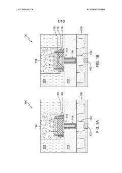
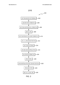
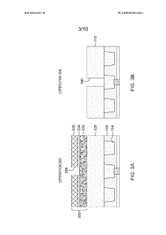
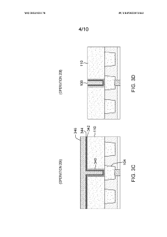
01 Scaling techniques for PCM cell structures
Various techniques are employed to scale down PCM cell structures while maintaining or improving performance. These include reducing the contact area between the phase change material and the heater, using confined cell structures, and implementing multi-layer phase change materials. These approaches help minimize the programming current required while increasing storage density, which is crucial for the commercial viability of PCM technology in high-density memory applications.- Scaling techniques for PCM cell structures: Various techniques are employed to scale down PCM cell structures while maintaining or improving performance. These include reducing the contact area between the phase change material and the heater, using confined cell structures, and implementing multi-level cell architectures. These scaling approaches help to reduce the programming current, improve thermal efficiency, and increase memory density while maintaining reliability.
- Material innovations for scaled PCM devices: Novel phase change materials and compositions are developed to enable further scaling of PCM devices. These materials include doped chalcogenides, composite materials with improved crystallization properties, and materials with lower melting points. These innovations help to reduce power consumption, improve cycling endurance, and enhance data retention in scaled PCM devices.
- Advanced PCM array architectures for scaling: Innovative array architectures are designed to facilitate PCM scaling. These include 3D stacking, crossbar arrays, and selector device integration. Such architectures enable higher memory density, improved thermal isolation between cells, and reduced cell-to-cell interference, which are critical for scaling PCM technology to smaller nodes.
- Control and programming schemes for scaled PCM: Specialized control and programming schemes are developed for scaled PCM devices. These include adaptive programming algorithms, precise current control methods, and temperature-compensated programming. These approaches help to maintain reliable operation, improve write/erase cycles, and ensure consistent performance as PCM cells are scaled down.
- System-level integration of scaled PCM: System-level approaches for integrating scaled PCM into computing architectures are developed. These include memory controllers optimized for PCM characteristics, hybrid memory systems combining PCM with other memory technologies, and specialized interfaces for PCM operation. These integration strategies help to leverage the benefits of scaled PCM while addressing its unique operational requirements.
02 Material engineering for improved PCM scaling
Advanced material engineering approaches are used to enhance PCM scaling capabilities. This includes developing doped chalcogenide materials, implementing composite phase change materials, and creating multi-layered structures with different thermal properties. These material innovations help reduce reset current, improve data retention, enhance endurance, and allow for further miniaturization of PCM cells while maintaining reliable switching characteristics.Expand Specific Solutions03 Architecture and integration solutions for PCM scaling
Novel memory architectures and integration techniques enable effective PCM scaling. These include 3D stacking of memory arrays, crossbar architectures, and innovative selector devices for high-density arrays. Integration solutions address challenges such as thermal crosstalk between adjacent cells, interconnect scaling, and compatibility with CMOS processes, allowing PCM technology to scale beyond the limitations of conventional memory technologies.Expand Specific Solutions04 Programming and read schemes for scaled PCM
Specialized programming and read schemes are developed to address the challenges of scaled PCM devices. These include multi-level cell programming techniques, adaptive programming algorithms that adjust pulse parameters based on cell characteristics, and sensing schemes that compensate for variability in scaled devices. These approaches enable reliable operation of highly scaled PCM cells while maintaining performance and endurance characteristics.Expand Specific Solutions05 System-level approaches for PCM scaling
System-level innovations support the scaling of PCM technology by addressing integration challenges with processors and other system components. These approaches include specialized memory controllers, hybrid memory systems that combine PCM with other memory technologies, and software techniques that optimize PCM usage patterns. System-level solutions help manage the trade-offs between performance, power consumption, and endurance in scaled PCM implementations.Expand Specific Solutions
Key Industry Players in PCM and Edge AI Ecosystem
The PCM (Phase Change Memory) technology for Edge AI accelerators is currently in an early growth phase, with significant market potential as edge computing expands. The market is projected to grow substantially as AI workloads increasingly move to edge devices, requiring memory solutions with lower latency and power consumption. Technologically, PCM is advancing toward maturity with key players driving innovation: Intel leads with commercial implementations, while academic institutions like Nanjing University of Posts & Telecommunications and Beijing University of Posts & Telecommunications contribute fundamental research. Memory manufacturers SK Hynix and TSMC are developing manufacturing capabilities, while specialized AI hardware companies like Rain Neuromorphics explore PCM's neuromorphic applications. The competitive landscape features established semiconductor giants collaborating with research institutions to overcome scaling challenges for next-generation edge AI deployments.
Intel Corp.
Technical Solution: Intel has developed a comprehensive PCM (Phase Change Memory) scaling roadmap for edge AI accelerators, focusing on their Optane technology. Their approach integrates PCM as both memory and computational elements in neuromorphic computing architectures. Intel's 3D XPoint technology enables high-density storage with multi-level cell capabilities, achieving up to 4 bits per cell in their latest iterations. For edge AI applications, Intel has demonstrated PCM-based in-memory computing that reduces the energy consumption by approximately 100x compared to conventional DRAM-based solutions. Their roadmap includes scaling PCM cell size down to sub-20nm technology nodes while maintaining reliability through advanced materials engineering and error correction techniques. Intel has also developed specialized programming algorithms that extend PCM endurance to over 10^7 cycles, addressing one of the key limitations of this technology for AI workloads.
Strengths: Mature manufacturing infrastructure, established ecosystem integration, and proven reliability in commercial products. Intel's vertical integration allows for optimized hardware-software co-design. Weaknesses: Higher power consumption compared to emerging alternatives, and scaling limitations at extreme nodes due to thermal crosstalk between adjacent cells.
SK hynix, Inc.
Technical Solution: SK hynix has pioneered a novel PCM architecture specifically designed for edge AI accelerators, focusing on ultra-low power operation and high-density integration. Their technology utilizes a proprietary chalcogenide material composition that enables faster crystallization and amorphization processes, reducing write latency by approximately 40% compared to conventional GST (Germanium-Antimony-Tellurium) compounds. SK hynix's scaling roadmap incorporates vertical stacking of PCM cells with dedicated selector devices, achieving bit densities exceeding 10 Gb/cm². For edge AI applications, they've developed specialized peripheral circuits that support in-memory vector-matrix multiplication operations, demonstrating energy efficiencies of less than 2 pJ per multiply-accumulate operation. Their roadmap projects scaling to 15nm feature sizes by 2025, with multi-level cell capabilities supporting 3-4 bits per cell while maintaining sufficient read margins for reliable inference operations in resource-constrained edge environments.
Strengths: Industry-leading cell-to-cell variability control, excellent retention characteristics at elevated temperatures common in edge devices, and advanced selector technology enabling high-density arrays. Weaknesses: Limited endurance compared to SRAM/DRAM alternatives, and relatively higher manufacturing costs due to specialized materials and processes.
Critical Patents and Research in PCM Scaling
Phase change memory cell with spacer
PatentWO2023021178A1
Innovation
- Incorporating a reactive-ion-etching-resistant material as a shield between the phase change material and the electrical insulator, and using a reactive-ion-etching-susceptible material for the guard, to protect the PCM material from damage during manufacturing processes while allowing selective etching.
Multi-layer phase change memory device
PatentWO2022142647A1
Innovation
- Multi-layer structure design for phase change memory (PCM) devices to enhance performance in analog computing for AI applications.
- Doping PCM materials with dielectrics and poorly electrically conductive materials (SiO2, SiO, SiON, SiOC, AlN) to increase crystallization temperature and resistivity.
- Tunable conductivity design enabling device-to-device variability control while maintaining high device resistance for minimal energy consumption.
Power Efficiency Considerations for PCM in Edge Devices
Power efficiency represents a critical factor in the deployment of Phase Change Memory (PCM) technology within edge AI accelerators. As edge devices typically operate under strict power constraints, PCM's energy profile must be carefully optimized to ensure viable implementation. Current PCM cells require significant energy for programming operations, with write operations consuming approximately 10-100 times more power than read operations.
The power consumption of PCM in edge applications can be categorized into three primary components: standby power, read power, and write power. Standby power, while relatively minimal compared to DRAM, still contributes to the overall energy budget. Read operations demonstrate favorable energy characteristics, consuming approximately 10-50 pJ per bit, making PCM particularly attractive for inference-heavy workloads where read operations dominate.
Write operations present the most significant power efficiency challenge, requiring 100-500 pJ per bit due to the thermal processes involved in phase transitions. This asymmetry between read and write energy demands necessitates architectural innovations that minimize write operations or distribute them strategically to prevent power spikes and thermal hotspots.
Recent advancements in PCM cell design have demonstrated promising improvements in power efficiency. Multi-level cell (MLC) configurations, while increasing density, introduce additional power challenges due to precise resistance control requirements. However, innovations in programming algorithms, including iterative programming schemes and adaptive pulse techniques, have reduced energy requirements by up to 40% compared to earlier PCM implementations.
Circuit-level optimizations present another avenue for power efficiency improvements. Charge-pump designs with enhanced efficiency, selective row activation mechanisms, and intelligent power gating techniques have collectively reduced peripheral circuit power consumption by 25-35% in recent prototype implementations. These improvements are particularly valuable for edge devices where every milliwatt of power consumption matters.
System-level power management strategies specifically tailored for PCM characteristics are emerging as crucial components in edge AI accelerator designs. Dynamic voltage and frequency scaling (DVFS) techniques adapted for PCM's unique characteristics can optimize power consumption based on workload demands. Additionally, workload-aware memory access scheduling algorithms that batch write operations during low-activity periods help maintain power consumption within acceptable limits.
Looking forward, the projected scaling roadmap for PCM in edge AI accelerators indicates potential for further power efficiency improvements through materials engineering and device structure innovations. Reduced contact area designs, novel phase change materials with lower melting points, and hybrid cell structures combining PCM with other memory technologies promise to reduce programming energy requirements by an additional 30-50% within the next three to five years.
Competitive Memory Technologies Assessment
In the landscape of memory technologies competing with Phase Change Memory (PCM) for edge AI accelerator applications, several alternatives present distinct advantages and limitations. SRAM continues to dominate as the primary on-chip memory solution due to its high speed and compatibility with standard CMOS processes. However, its scaling limitations and high leakage power consumption create opportunities for emerging technologies. DRAM offers higher density than SRAM but faces challenges in scaling below 10nm and requires periodic refresh operations that impact energy efficiency in edge devices.
Flash memory provides non-volatility and high density but suffers from slow write speeds and limited endurance, making it suboptimal for write-intensive AI workloads. Emerging as strong competitors to PCM, MRAM (Magnetic RAM) and ReRAM (Resistive RAM) each present unique value propositions. MRAM offers unlimited endurance, fast access times, and CMOS compatibility, with companies like Everspin and Samsung advancing its commercialization. However, MRAM currently faces challenges in achieving the density levels required for large-scale AI model storage.
ReRAM demonstrates excellent scaling potential and multi-level cell capabilities that align well with neural network weight storage requirements. Companies including Weebit Nano and Crossbar have made significant progress in ReRAM development, though challenges in resistance drift and variability persist. FeRAM (Ferroelectric RAM) offers another alternative with fast write speeds and low power consumption but faces integration and scaling difficulties.
When comparing these technologies against PCM for edge AI applications, several key metrics emerge as critical: write endurance, retention time, access latency, energy per bit, and integration complexity. PCM's advantages in non-volatility, endurance (compared to Flash), and density position it favorably for certain edge AI applications, particularly those requiring persistent weight storage with moderate update frequency.
The competitive landscape continues to evolve rapidly, with major memory manufacturers including Micron, Samsung, and Western Digital investing across multiple technologies rather than focusing exclusively on one solution. This hedging strategy suggests the industry anticipates different memory technologies finding specialized roles within the heterogeneous memory hierarchy of future edge AI systems, rather than a single technology emerging as dominant across all applications.
Unlock deeper insights with Patsnap Eureka Quick Research — get a full tech report to explore trends and direct your research. Try now!
Generate Your Research Report Instantly with AI Agent
Supercharge your innovation with Patsnap Eureka AI Agent Platform!