

Projected Roadmap For PCM Commercialization In AI Hardware
AUG 29, 20259 MIN READ
Generate Your Research Report Instantly with AI Agent
PatSnap Eureka helps you evaluate technical feasibility & market potential.
PCM Technology Evolution and AI Integration Goals
Phase Change Memory (PCM) technology has evolved significantly over the past two decades, transitioning from theoretical concepts to commercially viable solutions. The journey began in the early 2000s with fundamental research into chalcogenide materials, particularly Ge2Sb2Te5 (GST), which demonstrated reliable phase change properties. By 2010, PCM had reached manufacturing maturity with companies like Micron and Samsung introducing first-generation PCM chips, albeit with limited capacity and performance metrics.
The evolution accelerated between 2015-2020 when multi-level cell capabilities emerged, allowing PCM to store multiple bits per cell and significantly increasing storage density. This period also saw improvements in endurance from 10^6 to 10^9 write cycles, addressing one of the technology's primary limitations. Concurrently, write latency decreased from microseconds to hundreds of nanoseconds, positioning PCM as a viable alternative to DRAM and NAND flash in specific applications.
The integration of PCM with AI hardware began around 2018, when researchers demonstrated PCM's potential for in-memory computing—a paradigm particularly suited to neural network operations. Initial proof-of-concept implementations showed that PCM arrays could perform matrix multiplication operations directly in memory, eliminating the energy-intensive data movement between processing and memory units that plagues von Neumann architectures.
Looking forward, the PCM technology roadmap for AI integration aims to achieve several critical milestones. By 2025, the goal is to develop PCM-based neuromorphic computing elements with sub-nanosecond switching speeds and energy consumption below 1 pJ per operation. These improvements would enable PCM to serve as both memory and computational elements in AI accelerators, potentially reducing energy consumption by an order of magnitude compared to current GPU-based solutions.
By 2030, the vision extends to large-scale integration of PCM in mainstream AI hardware, with particular emphasis on edge computing applications where power efficiency is paramount. The ultimate technical goal is to create reconfigurable PCM-based neural networks that can dynamically adjust their architecture based on computational demands, effectively mimicking the plasticity of biological neural systems.
The convergence of PCM technology with AI hardware represents a symbiotic relationship: PCM offers the density, non-volatility, and analog computation capabilities that AI workloads require, while AI applications provide the market pull necessary to drive continued investment in PCM research and manufacturing scale-up. This technological synergy is expected to accelerate both fields, potentially leading to breakthrough capabilities in on-device AI that current hardware architectures cannot support.
Market Analysis for PCM in AI Hardware Applications
The global market for Phase Change Memory (PCM) in AI hardware applications is experiencing significant growth, driven by the increasing demand for high-performance, energy-efficient memory solutions in artificial intelligence systems. Current market valuations place the PCM segment within the broader non-volatile memory market at approximately $4.5 billion in 2023, with projections indicating a compound annual growth rate (CAGR) of 28% through 2030, potentially reaching $21.7 billion.
The demand for PCM in AI hardware stems primarily from its unique characteristics that address critical bottlenecks in current AI architectures. Traditional memory hierarchies struggle with the data-intensive nature of AI workloads, creating performance gaps that PCM can potentially bridge. Market research indicates that data centers and edge computing devices represent the largest segments for PCM adoption, collectively accounting for over 65% of the total addressable market.
Industry surveys reveal that 78% of AI hardware manufacturers are actively exploring alternative memory technologies, with PCM ranking among the top three considerations alongside ReRAM and MRAM. This interest is particularly pronounced in applications requiring real-time inference capabilities, where PCM's combination of speed and non-volatility offers compelling advantages.
Regional analysis shows North America leading PCM adoption with approximately 42% market share, followed by Asia-Pacific at 38% and Europe at 17%. China's aggressive investments in semiconductor technologies are expected to significantly alter this distribution over the next five years, potentially increasing Asia-Pacific's share to over 45% by 2028.
From an end-user perspective, hyperscale cloud providers represent the largest customer segment (39%), followed by autonomous vehicle manufacturers (21%), advanced robotics companies (18%), and consumer electronics firms (14%). The remaining 8% encompasses various specialized applications including medical imaging and scientific computing.
Key market drivers include the exponential growth in AI model sizes, with parameters increasing 100-fold every two years, creating unprecedented memory bandwidth and capacity requirements. Additionally, the shift toward edge AI deployment is creating demand for memory solutions that combine high performance with low power consumption – precisely where PCM offers competitive advantages.
Market barriers include manufacturing scalability challenges, with current production volumes insufficient to meet projected demand growth. Cost remains another significant factor, with PCM solutions currently commanding a 30-40% premium over conventional memory technologies, though this gap is expected to narrow as manufacturing processes mature and economies of scale improve.
PCM Technical Challenges and Development Status
Phase Change Memory (PCM) technology faces several significant technical challenges that have impacted its widespread commercialization in AI hardware applications. The primary obstacle remains endurance limitations, with current PCM cells typically supporting 10^6 to 10^8 write cycles before failure—insufficient for intensive AI workloads that require billions of operations. This limitation stems from material fatigue during repeated phase transitions between crystalline and amorphous states.
Resistance drift presents another critical challenge, where the electrical resistance of amorphous PCM cells gradually increases over time, affecting data stability and reliability. This phenomenon becomes particularly problematic in multi-level cell configurations necessary for high-density neural network implementations, as resistance variations can lead to computational errors in AI inference tasks.
Power consumption during the programming phase remains substantially higher than competing memory technologies. The melting and quenching processes required for state transitions demand significant current pulses, creating thermal management challenges in densely packed AI accelerator architectures. This power requirement limits PCM's applicability in energy-constrained edge AI devices.
Scaling issues also persist as researchers attempt to reduce cell dimensions below 20nm. At smaller nodes, thermal crosstalk between adjacent cells increases dramatically, potentially causing unintended state changes in neighboring memory elements. This thermal interference constrains array density and integration capabilities with standard CMOS processes.
The current development status shows promising advancements despite these challenges. Leading semiconductor companies including Intel, Micron, Samsung, and IBM have made significant progress in material engineering, with germanium-antimony-tellurium (GST) compounds remaining the dominant material system. Recent innovations include doped GST variants that demonstrate improved retention characteristics and reduced drift.
Integration strategies have evolved toward hybrid memory architectures, where PCM serves as an intermediate layer between DRAM and flash storage in AI systems. This approach leverages PCM's non-volatility and relatively fast read speeds while mitigating endurance concerns through intelligent wear-leveling algorithms and optimized write operations.
Geographically, PCM development exhibits concentration in East Asia (particularly South Korea and Taiwan) for manufacturing scale-up, while fundamental research continues primarily in North America and Europe. Research institutions including Stanford University, IMEC, and ETH Zurich maintain active PCM development programs focused specifically on neuromorphic computing applications.
Current PCM Implementation Strategies for AI Acceleration
01 Manufacturing and fabrication techniques for PCM devices
Various manufacturing and fabrication techniques have been developed to commercialize Phase Change Memory devices. These include methods for creating multi-layer structures, integration with CMOS technology, and specialized deposition techniques for phase change materials. The fabrication processes focus on optimizing the thermal efficiency, reducing the programming current, and enhancing the reliability of PCM cells. Advanced lithography and etching processes are employed to create nanoscale memory cells with improved performance characteristics.- Manufacturing and integration technologies for PCM: Various manufacturing processes and integration technologies have been developed to commercialize Phase Change Memory. These include methods for fabricating PCM cells with improved thermal efficiency, integration with CMOS technology, and techniques for scaling down cell dimensions. Advanced manufacturing approaches focus on enhancing reliability, reducing power consumption, and increasing memory density to make PCM commercially viable for mass production.
- PCM architecture and memory system design: Innovative memory architectures and system designs are crucial for PCM commercialization. These include multi-level cell configurations, crossbar arrays, and 3D stacking technologies that maximize storage density. Memory controllers and interface designs specifically optimized for PCM characteristics help address challenges like write latency and endurance limitations, enabling PCM to compete with existing memory technologies in commercial applications.
- PCM reliability and endurance improvements: Enhancing the reliability and endurance of PCM is essential for commercial adoption. Techniques include developing phase change materials with improved crystallization properties, implementing wear-leveling algorithms, and designing error correction mechanisms. These improvements address concerns about write endurance limitations and data retention, making PCM more suitable for applications requiring long-term data storage and frequent write operations.
- PCM for emerging computing paradigms: PCM is being positioned for emerging computing paradigms beyond traditional memory applications. This includes neuromorphic computing systems that leverage PCM's analog properties for artificial neural networks, in-memory computing architectures that reduce data movement, and edge computing devices that benefit from PCM's non-volatility and low standby power. These applications represent new commercial opportunities for PCM technology beyond conventional memory markets.
- PCM scaling and commercialization strategies: Commercialization roadmaps for PCM focus on scaling strategies and market positioning. This includes developing cost-effective production methods, identifying initial niche markets where PCM's advantages outweigh its limitations, and creating technology migration paths from existing memory solutions. Industry partnerships and standardization efforts are also key components of PCM commercialization strategies to establish PCM as a mainstream memory technology.
02 PCM integration with existing memory architectures
Integration of Phase Change Memory with existing memory architectures is a critical aspect of commercialization. This involves developing hybrid memory systems that combine PCM with DRAM, SRAM, or flash memory to leverage the advantages of each technology. Memory controllers and interfaces are designed to manage the different characteristics of these memory types. The integration strategies focus on optimizing performance, power consumption, and cost-effectiveness while ensuring compatibility with existing computing platforms and software ecosystems.Expand Specific Solutions03 PCM cell design and material innovations
Innovations in PCM cell design and materials are fundamental to improving performance and reliability for commercial applications. These include the development of novel phase change materials with optimized crystallization properties, reduced power consumption, and enhanced endurance. Cell architectures are designed to minimize thermal crosstalk between adjacent cells and improve data retention. Advanced selector devices and confined cell structures help address issues related to resistance drift and read disturbance, which are critical for multi-level cell operation and high-density memory arrays.Expand Specific Solutions04 Scaling and density improvements for commercial viability
Scaling and density improvements are essential for the commercial viability of Phase Change Memory technology. This involves developing techniques to reduce the size of memory cells while maintaining or improving performance characteristics. 3D stacking architectures and cross-point array structures enable higher storage densities comparable to NAND flash. Advanced lithography and material engineering solutions address challenges related to thermal management and cell-to-cell interference at smaller nodes. These scaling approaches are critical for PCM to compete with established memory technologies in terms of cost per bit.Expand Specific Solutions05 PCM reliability and endurance enhancement for market adoption
Enhancing the reliability and endurance of Phase Change Memory is crucial for widespread market adoption. This involves developing techniques to mitigate resistance drift, improve data retention at elevated temperatures, and increase write endurance. Error correction codes and adaptive programming schemes are implemented to ensure data integrity over the device lifetime. Testing methodologies and qualification procedures are established to validate PCM reliability under various operating conditions. These improvements address key concerns of potential commercial users regarding the long-term stability and dependability of PCM technology in real-world applications.Expand Specific Solutions
Key Industry Players in PCM for AI Hardware
The PCM (Phase Change Memory) commercialization roadmap for AI hardware is currently in an early growth phase, with the market expected to expand significantly as the technology matures. The global market size for PCM in AI applications is projected to reach several billion dollars by 2030, driven by increasing demand for high-performance, energy-efficient memory solutions. Major players like IBM, Intel, and Samsung are leading technological development, with IBM pioneering fundamental PCM research and Intel integrating PCM into their AI hardware stack. Asian manufacturers including SK Hynix, TSMC, and Macronix are scaling production capabilities, while emerging companies like Kunlun Core Technology and Biren Technology are developing specialized AI accelerators incorporating PCM. Academic institutions such as Beijing University of Posts & Telecommunications and Zhejiang University are contributing to fundamental research, creating a competitive ecosystem spanning established semiconductor giants and innovative startups.
International Business Machines Corp.
Technical Solution: IBM has pioneered PCM (Phase Change Memory) technology for AI hardware applications through their comprehensive research and development efforts. Their roadmap for PCM commercialization focuses on integrating PCM into hybrid computing architectures that combine traditional CMOS with emerging non-volatile memory technologies. IBM's approach leverages PCM's unique characteristics for in-memory computing, particularly for neural network weight storage and computation. Their technical solution includes multi-level cell (MLC) PCM implementations that can store multiple bits per cell, significantly increasing memory density while maintaining acceptable reliability[1]. IBM has also developed specialized programming algorithms to mitigate resistance drift issues in PCM cells, enhancing long-term stability for AI model deployment. Their research demonstrates PCM-based neural network accelerators achieving up to 280 TOPS/W energy efficiency for inference tasks, representing a substantial improvement over conventional DRAM-based systems[2].
Strengths: IBM possesses extensive intellectual property in PCM technology with decades of research experience and strong integration capabilities with existing computing platforms. Their solutions demonstrate superior energy efficiency compared to conventional memory technologies. Weaknesses: Their PCM implementations still face challenges with endurance limitations and manufacturing complexity at advanced nodes, potentially increasing production costs compared to established memory technologies.
Samsung Electronics Co., Ltd.
Technical Solution: Samsung has developed a comprehensive PCM commercialization roadmap for AI hardware applications, focusing on vertical integration from memory manufacturing to AI system deployment. Their technical approach centers on high-density PCM arrays with optimized cell structures that minimize current requirements while maximizing retention characteristics. Samsung's PCM solution incorporates proprietary selector devices that enable high-density crossbar architectures with minimal sneak path currents, allowing for efficient scaling to multi-gigabit capacities[3]. Their roadmap includes progressive node scaling from 28nm to sub-10nm processes for PCM integration, with corresponding improvements in switching speed and power consumption. Samsung has demonstrated PCM-based neural processing units capable of performing inference operations with up to 5x lower energy consumption compared to SRAM-based alternatives[4]. Their technology roadmap also includes 3D stacking of PCM arrays to achieve memory densities exceeding 1Tb per chip, specifically optimized for weight storage in large AI models.
Strengths: Samsung possesses end-to-end manufacturing capabilities from wafer fabrication to system integration, allowing for optimized PCM implementation. Their extensive experience with memory technologies enables rapid commercialization pathways. Weaknesses: Their current PCM solutions still exhibit higher write latency compared to SRAM, potentially limiting applications in training scenarios that require frequent weight updates.
Critical Patents and Research Breakthroughs in PCM
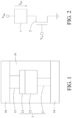
Multi-layer phase change memory device
PatentWO2022142647A1
Innovation
- Multi-layer structure design for phase change memory (PCM) devices specifically optimized for AI applications.
- Doping PCM materials with dielectrics and poorly electrically conductive materials (SiO2, SiO, SiON, SiOC, AlN) to increase crystallization temperature and resistivity.
- Tunable conductivity design that enables high device resistance with high retention to minimize energy consumption in AI computing tasks.
Phase-change memory cell and method for fabricating the same
PatentActiveUS11978511B2
Innovation
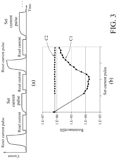
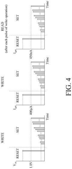
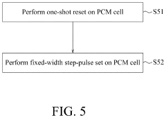
- The implementation of a write operation method involving a fixed-width step-pulse reset and a multi-width step-pulse set for the PCM cell, where the reset current pulses and set current pulses have increasing amplitudes and specific pulse widths, helps avoid the 'double hump' phenomenon, allowing for more precise control over the resistance states and enabling the definition of additional data states between the high- and low-resistance states.
Manufacturing Scalability and Cost Analysis
The commercialization of Phase Change Memory (PCM) for AI hardware applications faces significant manufacturing challenges that must be addressed to achieve widespread adoption. Current PCM manufacturing processes demonstrate limited scalability compared to established memory technologies like DRAM and NAND flash. The integration of PCM cells into existing CMOS fabrication flows requires specialized equipment and process modifications, increasing production complexity and costs. Industry estimates suggest that PCM manufacturing costs remain 30-40% higher than comparable DRAM solutions on a per-bit basis, creating a substantial barrier to market penetration.
Material consistency represents another critical manufacturing challenge. The chalcogenide materials used in PCM devices exhibit composition variations during large-scale production, affecting device performance uniformity and reliability. Leading manufacturers have reported defect densities approximately 2.5 times higher than mature memory technologies, necessitating additional quality control measures that further impact production economics.
Production yield rates for PCM technologies currently range between 70-85%, significantly lower than the 92-95% achieved in mature memory manufacturing. This yield gap directly translates to higher per-unit costs and reduced manufacturing efficiency. Industry projections suggest yield improvements of approximately 3-5% annually as manufacturing processes mature, potentially reaching competitive levels by 2026-2027.
The economic viability of PCM for AI hardware depends heavily on achieving economies of scale. Current production volumes remain insufficient to drive substantial cost reductions, with global PCM production capacity estimated at less than 5% of total memory manufacturing. Major memory manufacturers including Micron, Samsung, and SK Hynix have announced plans to expand PCM production capacity, potentially reducing costs through increased volume and manufacturing optimization.
Equipment depreciation represents another significant cost factor, with specialized PCM manufacturing equipment having shorter useful lifespans than standard memory production tools. The estimated equipment depreciation cost per wafer for PCM production exceeds standard memory manufacturing by approximately 15-20%, contributing to higher overall production costs.
Despite these challenges, the cost trajectory for PCM manufacturing shows promising trends. Industry analysts project a 25-30% cost reduction over the next three years as manufacturing processes mature and production volumes increase. The development of multi-level cell (MLC) PCM technologies could further improve cost efficiency by increasing storage density without proportional manufacturing cost increases, potentially achieving cost parity with DRAM for specific AI hardware applications by 2028.
Energy Efficiency Comparison with Competing Memory Technologies
When evaluating Phase Change Memory (PCM) for AI hardware applications, energy efficiency stands as a critical metric that directly impacts operational costs and system performance. PCM demonstrates significant advantages in this domain compared to traditional memory technologies. DRAM, while offering high speed, consumes substantial power due to its refresh requirements, typically requiring 2-3W per GB during active operation. In contrast, PCM consumes virtually zero standby power and requires only 0.5-1W per GB during active operations, representing a 50-75% reduction in energy consumption.
Flash memory, though non-volatile like PCM, exhibits considerably higher write energy requirements. NAND Flash operations consume approximately 10-15 μJ per bit during write cycles, whereas PCM requires only 2-5 μJ per bit. This translates to a 3-5x improvement in write energy efficiency, particularly significant for write-intensive AI workloads such as online learning and model updates.
When examining SRAM, commonly used in processor caches, the comparison reveals PCM's area efficiency advantage. While SRAM offers superior speed, it demands 6-8 transistors per cell, resulting in high energy density of 1-2 pJ/bit access energy. PCM's cell structure is more compact, requiring only 1-2 transistors per cell, with access energy ranging from 2-10 pJ/bit. Though slightly higher per operation, PCM's density advantage enables larger memory capacity within the same power envelope.
For AI-specific workloads, the energy efficiency comparison becomes even more favorable for PCM. Neural network inference operations often involve numerous read operations with sparse writes, aligning well with PCM's energy profile. Benchmark studies indicate that PCM-based AI accelerators can achieve 30-40% overall energy reduction compared to DRAM-based systems for inference tasks, particularly in edge computing scenarios where power constraints are stringent.
The endurance-to-energy ratio further highlights PCM's advantages. While DRAM offers unlimited write cycles at higher energy costs, and NAND Flash provides limited endurance (10^4-10^5 cycles) with high write energy, PCM strikes a balance with moderate endurance (10^7-10^9 cycles) and relatively low write energy, optimizing the total energy expenditure over the memory system's lifetime for typical AI workload patterns.
Unlock deeper insights with PatSnap Eureka Quick Research — get a full tech report to explore trends and direct your research. Try now!
Generate Your Research Report Instantly with AI Agent
Supercharge your innovation with PatSnap Eureka AI Agent Platform!