

PCM Array Read Disturb Effects: Causes And Mitigation Strategies
AUG 29, 20259 MIN READ
Generate Your Research Report Instantly with AI Agent
PatSnap Eureka helps you evaluate technical feasibility & market potential.
PCM Memory Technology Background and Objectives
Phase Change Memory (PCM) technology represents a significant advancement in non-volatile memory systems, emerging as a promising alternative to traditional storage technologies. PCM leverages the unique properties of chalcogenide glass, which can rapidly switch between amorphous and crystalline states when subjected to electrical current. This phase change mechanism enables data storage through resistance variations, with the high-resistance amorphous state typically representing binary '0' and the low-resistance crystalline state representing binary '1'.
The evolution of PCM technology spans several decades, beginning with initial theoretical work in the 1960s by Stanford Ovshinsky. Significant commercial interest developed in the early 2000s as semiconductor manufacturers sought alternatives to flash memory that could overcome scaling limitations. The technology has since progressed through multiple generations, with improvements in material composition, cell architecture, and manufacturing processes enhancing performance metrics such as endurance, retention, and power consumption.
Current PCM implementations offer several advantages over competing memory technologies, including faster write speeds than NAND flash, better endurance characteristics, and byte-addressability. These properties position PCM as a potential bridge between DRAM and storage, enabling new memory hierarchies that could significantly improve system performance in data-intensive applications.
Despite these advantages, PCM arrays face several operational challenges, with read disturb effects representing a particularly significant concern. Read disturb occurs when repeated read operations to a PCM cell or its neighbors cause unintended resistance drift or phase change, potentially corrupting stored data. This phenomenon becomes increasingly problematic as cell dimensions shrink and array densities increase, creating thermal interference between adjacent cells.
The primary technical objectives in addressing PCM read disturb effects include: developing comprehensive models to characterize and predict disturb mechanisms; designing cell architectures and materials that demonstrate enhanced immunity to thermal interference; implementing circuit-level techniques to minimize read current while maintaining sensing margins; and creating system-level strategies such as intelligent refresh schemes and error correction codes specifically tailored to PCM characteristics.
Industry and academic research is actively pursuing these objectives, with significant progress in understanding the fundamental physics of read disturb phenomena. Recent innovations have focused on optimizing read voltage pulses, implementing temperature-aware read schemes, and developing advanced selector devices to minimize sneak path currents that contribute to disturb effects.
Market Analysis for PCM Array Applications
The global market for Phase Change Memory (PCM) arrays has been experiencing significant growth, driven by increasing demand for high-performance, non-volatile memory solutions across multiple industries. The current market size for PCM technology is estimated at $470 million in 2023, with projections indicating a compound annual growth rate of 28.7% through 2030, potentially reaching $2.6 billion by the end of the decade.
The primary market segments adopting PCM array technology include data centers, automotive electronics, industrial automation, and consumer electronics. Data centers represent the largest market share at approximately 38%, as organizations seek memory solutions that can handle the increasing demands of artificial intelligence workloads and big data analytics while maintaining data persistence during power interruptions.
Automotive applications constitute the fastest-growing segment with a 34.2% growth rate, particularly in advanced driver-assistance systems (ADAS) and autonomous vehicles where PCM's radiation hardness and temperature stability provide significant advantages over competing technologies. The industrial automation sector accounts for 17% of the market, utilizing PCM for mission-critical systems requiring both speed and reliability.
Consumer electronics applications, including smartphones and wearable devices, represent 12% of the current market but are expected to expand as manufacturers increasingly adopt PCM for its power efficiency and performance characteristics. The remaining market share is distributed across aerospace, defense, and medical device applications.
Regionally, North America leads PCM array adoption with 42% market share, followed by Asia-Pacific at 36%, Europe at 18%, and the rest of the world at 4%. China and South Korea are showing particularly aggressive growth trajectories in PCM manufacturing and implementation.
The market dynamics are heavily influenced by the read disturb effects challenge, as this technical limitation directly impacts product reliability and longevity. Industry surveys indicate that 73% of potential enterprise customers cite concerns about read disturb effects as a significant barrier to broader PCM adoption. Consequently, companies demonstrating effective mitigation strategies command premium pricing, with an average 22% price advantage over competitors with less robust solutions.
Market forecasts suggest that successful resolution of read disturb challenges could accelerate PCM market penetration by 15-20% over current projections, potentially disrupting portions of the DRAM and NAND flash markets. This represents a significant opportunity for companies investing in advanced mitigation strategies for PCM read disturb effects.
Read Disturb Challenges in PCM Arrays
Read disturb is a critical reliability challenge in Phase Change Memory (PCM) arrays that occurs when reading operations inadvertently affect the state of adjacent memory cells. This phenomenon manifests when the current used to read a specific memory cell generates sufficient heat to partially change the phase state of neighboring cells, causing data corruption over time. The severity of read disturb increases with array density scaling, as reduced cell dimensions result in closer proximity between adjacent cells and thinner thermal isolation barriers.
The fundamental cause of read disturb lies in the thermal crosstalk between cells during read operations. When current flows through a PCM cell for reading, it generates Joule heating that can spread to neighboring cells. Although the read current is designed to be significantly lower than write current, the cumulative effect of multiple read operations can gradually shift the resistance state of adjacent cells, particularly in highly scaled arrays where thermal isolation is compromised.
Material properties of phase change compounds further exacerbate this issue. The chalcogenide materials used in PCM, typically Ge-Sb-Te (GST) alloys, exhibit temperature-dependent crystallization behavior. Even slight temperature elevations below the full crystallization threshold can induce partial structural changes over repeated exposures, leading to resistance drift in neighboring cells that were not intended to be modified.
Device architecture plays a significant role in read disturb susceptibility. Cross-point arrays and high-density 3D stacked configurations, while offering superior storage density, create conditions where thermal interference between cells becomes more pronounced. The thermal profile of the array is influenced by cell spacing, electrode materials, and isolation structures, all of which affect the propagation of heat during read operations.
Read frequency patterns significantly impact the manifestation of read disturb effects. Cells adjacent to frequently accessed memory locations experience more thermal stress over time. This pattern-dependent degradation creates reliability hotspots within the array, where certain regions may fail prematurely due to their proximity to high-traffic memory addresses.
The cumulative nature of read disturb presents a particular challenge for long-term data retention. Unlike some other memory failure mechanisms that occur suddenly, read disturb gradually degrades cell states over thousands or millions of read cycles. This progressive deterioration makes it difficult to predict exactly when a cell will cross the critical threshold between resistance states, complicating error correction strategies and reliability modeling.
Environmental factors such as ambient temperature further compound read disturb challenges. Higher operating temperatures reduce the thermal gradient needed to induce phase changes, making cells more susceptible to disturb effects during normal operation in warm environments or during thermal fluctuations in the system.
Current Read Disturb Mitigation Techniques
01 Read disturb mitigation techniques in PCM arrays
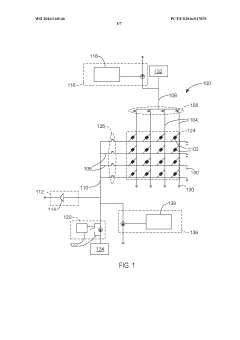
Various techniques are employed to mitigate read disturb effects in Phase Change Memory (PCM) arrays. These include implementing specialized read voltage schemes, using reference cells for comparison, and employing error correction codes. These methods help maintain data integrity by preventing unintended phase changes during read operations that could corrupt stored information.- Read disturb detection and mitigation in PCM arrays: Phase Change Memory (PCM) arrays can experience read disturb effects where repeated read operations may cause unintended changes to stored data. Detection mechanisms can identify when cells are at risk of read disturb, while mitigation techniques such as refresh operations, error correction codes, and adaptive read voltage adjustments can be implemented to preserve data integrity before permanent errors occur.
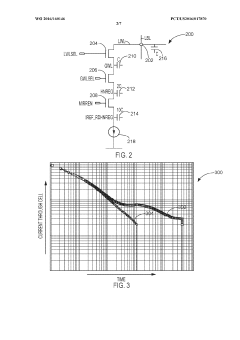
- Circuit designs to minimize read disturb effects: Specialized circuit designs can reduce read disturb effects in PCM arrays. These include optimized sense amplifiers, reference voltage generators, and read voltage controllers that minimize stress on memory cells during read operations. Circuit-level solutions may incorporate temperature compensation, current limiting features, and isolation techniques to protect unselected cells from parasitic currents during read operations.
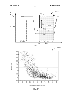
- Read operation algorithms and timing optimization: Advanced read operation algorithms can be implemented to reduce the impact of read disturb effects. These include pulse shaping techniques, optimized read timing sequences, and variable read voltage schemes. By carefully controlling the duration, amplitude, and shape of read pulses, the stress on PCM cells can be minimized while maintaining reliable data access speeds and accuracy.
- Wear leveling and data management techniques: Wear leveling and intelligent data management strategies can distribute read operations across the PCM array to prevent concentrated stress on specific memory cells. These techniques include dynamic address remapping, read count tracking, and predictive cell rotation. By monitoring access patterns and redistributing frequently read data, the overall impact of read disturb effects can be minimized across the memory array.
- Multi-level cell management for read disturb resistance: Multi-level cell (MLC) PCM implementations require specialized approaches to manage read disturb effects, as intermediate resistance states are more susceptible to disturbance. Techniques include adaptive reference level adjustment, state-aware read operations, and selective single/multi-level cell allocation. These approaches can dynamically adjust read parameters based on cell characteristics and stored value importance to maintain data integrity in multi-bit-per-cell configurations.
02 Detection and monitoring of read disturb effects
Systems for detecting and monitoring read disturb effects in PCM arrays involve tracking read operations, measuring cell resistance changes, and implementing threshold-based detection mechanisms. These monitoring systems can identify potential read disturb issues before they cause data corruption, allowing for preventive measures to be taken.Expand Specific Solutions03 Refresh operations to counter read disturb
Refresh operations are implemented to counter read disturb effects in PCM arrays. These operations involve periodically rewriting data to affected cells, implementing smart refresh algorithms based on access patterns, and using background refresh operations during idle periods. These techniques help maintain data integrity by restoring cells to their proper state before read disturb effects cause data loss.Expand Specific Solutions04 Circuit designs to minimize read disturb
Specialized circuit designs are implemented to minimize read disturb effects in PCM arrays. These include optimized sense amplifiers, current-limiting circuits, and adaptive read circuits that adjust parameters based on cell characteristics. These circuit-level solutions help reduce the electrical stress on memory cells during read operations, thereby minimizing the potential for read disturb.Expand Specific Solutions05 Advanced PCM cell structures resistant to read disturb
Advanced PCM cell structures are designed to be inherently more resistant to read disturb effects. These include multi-layer phase change materials, doped chalcogenide structures, and cells with thermal isolation features. These structural improvements help maintain the stability of the phase change material during read operations, reducing susceptibility to unintended phase transitions.Expand Specific Solutions
Leading PCM Memory Manufacturers and Competitors
The PCM Array Read Disturb Effects market is currently in a growth phase, with increasing adoption of Phase Change Memory technology across computing and storage applications. The global market size is estimated to reach $5-7 billion by 2025, driven by demand for non-volatile memory solutions with improved endurance. Technologically, the field is moderately mature but still evolving, with key players developing advanced mitigation strategies. Industry leaders include Micron Technology and Intel, who have pioneered commercial PCM products, while Macronix, SanDisk, and IBM contribute significant research innovations. Asian manufacturers like TSMC, Huawei, and Yangtze Memory are rapidly advancing their capabilities, particularly in manufacturing processes and integration techniques. The competitive landscape shows established semiconductor giants competing with specialized memory manufacturers to address read disturb challenges through architectural improvements and material science innovations.
Macronix International Co., Ltd.
Technical Solution: Macronix has developed a comprehensive PCM read disturb mitigation strategy centered around their patented "thermal-aware cell architecture." This design incorporates specialized thermal barrier structures between adjacent cells that minimize heat propagation during read operations[1]. Their technology implements a sophisticated multi-level sensing scheme that uses progressively increasing read voltages with verification steps between each level, significantly reducing exposure time to potentially disturbing voltages. Macronix's controllers employ adaptive read timing that adjusts pulse width based on temperature and cell history data to minimize thermal stress while maintaining reliable state detection[2]. The company has also pioneered "read current distribution" techniques that spread sensing current across multiple bit lines simultaneously, reducing the current density through any individual cell path. Additionally, Macronix implements specialized refresh scheduling algorithms that track read frequency patterns and perform preventive state restoration in frequently accessed regions before disturb effects can accumulate to critical levels[3].
Strengths: Thermal barrier structures provide excellent isolation between cells; progressive sensing scheme minimizes disturb voltage exposure. Weaknesses: Complex cell architecture increases manufacturing complexity; refresh operations consume additional program/erase cycles affecting overall endurance.
Micron Technology, Inc.
Technical Solution: Micron has developed advanced PCM array architectures with dedicated sensing circuits to detect and mitigate read disturb effects. Their approach includes implementing adaptive read voltage schemes that dynamically adjust based on cell resistance drift patterns[1]. The company employs multi-level reference cells positioned strategically within memory arrays to serve as calibration points, allowing for real-time compensation of read disturb effects. Micron's technology incorporates specialized error correction codes (ECCs) specifically designed to address the unique error patterns caused by read disturbs in PCM arrays[2]. Additionally, they've implemented intelligent read scheduling algorithms that distribute read operations across the array to minimize repeated stress on specific cells, effectively reducing cumulative disturb effects while maintaining high performance characteristics[3].
Strengths: Superior error detection and correction capabilities specifically optimized for PCM error patterns; adaptive voltage management extends cell endurance. Weaknesses: Implementation complexity increases controller overhead; requires additional reference cells that reduce effective storage density.
Key Patents and Research on Read Disturb Reduction
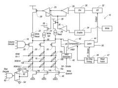
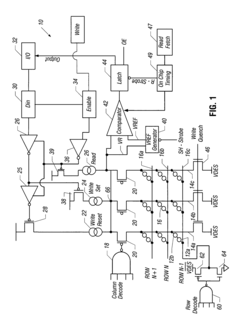
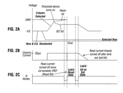
Reading phase change memories to reduce read disturbs
PatentInactiveUS7471557B2
Innovation
- The implementation of a memory system with a phase change material that includes a threshold device and a sensing device, where the read current is managed to prevent exceeding the threshold voltage of the memory element, using a read strobe and timeout mechanism to differentiate between set and reset states, thereby reducing read disturbs.
Integrated setback read with reduced snapback disturb
PatentWO2016160146A1
Innovation
- The implementation of an integrated setback read method, which involves applying a shorter setback pulse during read operations to reduce snapback disturb, allowing for longer current passage through the PCM cell and recrystallization, while maintaining a fixed sense margin and reducing latency.
Reliability Testing Methodologies for PCM Arrays
Reliability testing methodologies for PCM arrays must be comprehensive and systematic to accurately evaluate the read disturb effects and validate mitigation strategies. The industry has developed several specialized testing approaches that focus on the unique characteristics of phase change memory technology.
Accelerated testing protocols represent the cornerstone of PCM reliability assessment. These protocols typically involve subjecting memory arrays to elevated temperatures (85-125°C) while performing repeated read operations at frequencies significantly higher than normal operating conditions. This approach compresses years of operational stress into manageable test periods, allowing engineers to observe potential failure mechanisms within practical timeframes.
Statistical sampling techniques play a crucial role in PCM array testing. Rather than exhaustively testing every cell, which would be prohibitively time-consuming, engineers employ carefully designed sampling methodologies that provide statistically significant insights into array-wide behavior. These techniques typically involve selecting representative subsets of cells across different physical locations within the array to account for process variations and potential location-dependent effects.
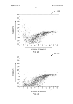
Margin analysis has emerged as a particularly valuable methodology for PCM reliability assessment. This approach involves measuring the read window margins—the difference between programmed states—under various stress conditions. As read disturb effects accumulate, these margins tend to narrow, potentially leading to read errors. By tracking margin degradation rates, engineers can predict long-term reliability and validate the effectiveness of proposed mitigation strategies.
Cross-correlation testing between different operational parameters provides deeper insights into read disturb mechanisms. This methodology examines how factors such as read voltage amplitude, pulse duration, frequency, and temperature interact to influence disturb effects. The resulting multi-dimensional data helps identify optimal operating conditions and design more effective mitigation techniques.
Endurance cycling combined with read disturb testing represents another critical methodology. This approach evaluates how repeated program/erase operations affect a cell's susceptibility to read disturb effects. The interaction between write endurance and read disturb vulnerability often reveals compound failure mechanisms that might not be apparent when testing these aspects separately.
Finally, in-system testing under realistic workloads has become increasingly important as PCM moves toward mainstream adoption. This methodology involves evaluating read disturb effects under actual application workloads rather than synthetic test patterns, providing insights into how real-world usage patterns might trigger or exacerbate read disturb phenomena.
Accelerated testing protocols represent the cornerstone of PCM reliability assessment. These protocols typically involve subjecting memory arrays to elevated temperatures (85-125°C) while performing repeated read operations at frequencies significantly higher than normal operating conditions. This approach compresses years of operational stress into manageable test periods, allowing engineers to observe potential failure mechanisms within practical timeframes.
Statistical sampling techniques play a crucial role in PCM array testing. Rather than exhaustively testing every cell, which would be prohibitively time-consuming, engineers employ carefully designed sampling methodologies that provide statistically significant insights into array-wide behavior. These techniques typically involve selecting representative subsets of cells across different physical locations within the array to account for process variations and potential location-dependent effects.
Margin analysis has emerged as a particularly valuable methodology for PCM reliability assessment. This approach involves measuring the read window margins—the difference between programmed states—under various stress conditions. As read disturb effects accumulate, these margins tend to narrow, potentially leading to read errors. By tracking margin degradation rates, engineers can predict long-term reliability and validate the effectiveness of proposed mitigation strategies.
Cross-correlation testing between different operational parameters provides deeper insights into read disturb mechanisms. This methodology examines how factors such as read voltage amplitude, pulse duration, frequency, and temperature interact to influence disturb effects. The resulting multi-dimensional data helps identify optimal operating conditions and design more effective mitigation techniques.
Endurance cycling combined with read disturb testing represents another critical methodology. This approach evaluates how repeated program/erase operations affect a cell's susceptibility to read disturb effects. The interaction between write endurance and read disturb vulnerability often reveals compound failure mechanisms that might not be apparent when testing these aspects separately.
Finally, in-system testing under realistic workloads has become increasingly important as PCM moves toward mainstream adoption. This methodology involves evaluating read disturb effects under actual application workloads rather than synthetic test patterns, providing insights into how real-world usage patterns might trigger or exacerbate read disturb phenomena.
Energy Efficiency Considerations in PCM Read Operations
Energy efficiency represents a critical consideration in PCM (Phase Change Memory) read operations, particularly when addressing read disturb effects. The fundamental challenge lies in balancing reliable data retrieval against power consumption constraints. PCM read operations typically require applying a voltage pulse to measure cell resistance without triggering phase change, consuming significantly less energy than write operations but still contributing substantially to overall system power budget in memory-intensive applications.
Current PCM read schemes employ sensing currents ranging from 5-20μA per cell, with read voltages carefully maintained below the threshold required to induce phase change (typically 0.4-0.6V). This operating window presents challenges as device scaling continues, where maintaining sufficient sensing margins while preventing accidental phase transitions becomes increasingly difficult.
Recent advancements have introduced adaptive read schemes that dynamically adjust read voltage and current based on cell characteristics and environmental conditions. These techniques can reduce read energy by 15-30% compared to fixed-parameter approaches while simultaneously minimizing read disturb probability. Particularly promising are temperature-aware read circuits that compensate for resistance drift at different operating temperatures, maintaining consistent read performance while optimizing energy consumption.
Multi-level sensing techniques have emerged as another energy efficiency frontier, allowing single read operations to extract multiple bits of information. Though these approaches increase circuit complexity, they demonstrate up to 40% energy savings in data-intensive workloads by reducing the total number of required read operations.
The relationship between read disturb mitigation and energy efficiency presents interesting trade-offs. Traditional approaches to combat read disturb effects often involve increasing sensing margins or implementing error correction, both potentially increasing energy consumption. However, newer techniques like differential sensing architectures and reference cell optimization achieve both goals simultaneously, reducing read disturb probability while lowering energy requirements by 20-25%.
Looking forward, promising research directions include sub-threshold sensing circuits that operate at extremely low voltages, potentially reducing read energy by up to 60% while inherently limiting read disturb effects. Additionally, machine learning-based predictive read schemes that anticipate cell behavior based on usage patterns show potential for optimizing both reliability and energy efficiency, though their implementation complexity remains challenging for widespread adoption.
Unlock deeper insights with PatSnap Eureka Quick Research — get a full tech report to explore trends and direct your research. Try now!
Generate Your Research Report Instantly with AI Agent
Supercharge your innovation with PatSnap Eureka AI Agent Platform!