Projected Manufacturing Cost Trends For PCM Technology Nodes
AUG 29, 20259 MIN READ
Generate Your Research Report Instantly with AI Agent
Patsnap Eureka helps you evaluate technical feasibility & market potential.
PCM Technology Evolution and Cost Objectives
Phase Change Memory (PCM) technology has evolved significantly since its conceptualization in the 1960s, transitioning from theoretical research to commercial applications. The evolution trajectory shows a clear pattern of increasing storage density, improved endurance cycles, and enhanced data retention capabilities. Current PCM nodes operate at 45-28nm, with industry leaders pushing toward 20nm and below to compete with established memory technologies like NAND Flash and DRAM.
The cost objectives for PCM technology development focus primarily on achieving manufacturing economies of scale while maintaining performance advantages. Historical cost trends indicate that PCM has followed a modified version of Moore's Law, with manufacturing costs decreasing approximately 30% with each node shrink, though this rate has slowed in recent generations due to increasing process complexity.
Material innovation represents a critical factor in PCM cost reduction. Traditional GST (Germanium-Antimony-Tellurium) compounds are being supplemented or replaced by alternative chalcogenide materials that offer better thermal stability and lower power consumption. These new materials aim to reduce the energy required for phase transitions, directly impacting manufacturing yields and operational costs.
Process optimization has emerged as another significant cost driver. Advanced deposition techniques like Atomic Layer Deposition (ALD) are replacing conventional Physical Vapor Deposition (PVD) methods, enabling more precise material control and higher yields. Integration of PCM cells with selector devices has also evolved, moving from traditional transistor-based selectors to more space-efficient diode and ovonic threshold switch (OTS) selectors, contributing to smaller die sizes and lower per-bit costs.
Equipment depreciation represents approximately 30-40% of PCM manufacturing costs, with material costs accounting for 20-25% and labor/overhead comprising the remainder. Industry projections suggest that as production volumes increase, these proportions will shift, with equipment costs becoming more distributed across larger production runs.
The cost objectives for future PCM nodes (sub-20nm) include achieving a manufacturing cost of less than $0.10 per gigabyte by 2025, making PCM competitive with high-performance NAND Flash. This requires innovations in lithography techniques, materials science, and process integration. Multi-level cell (MLC) and potentially quad-level cell (QLC) architectures are being explored to increase bit density without proportional increases in manufacturing complexity.
Cross-point array architectures represent another avenue for cost reduction, potentially increasing memory density by 30-50% compared to conventional designs. These architectures, combined with 3D stacking technologies, aim to maximize the number of bits per unit area, directly reducing the cost per bit while maintaining PCM's performance advantages in terms of speed and endurance.
Market Demand Analysis for PCM Manufacturing
The global market for Phase Change Memory (PCM) manufacturing is experiencing significant growth driven by increasing demand for high-performance, non-volatile memory solutions. Current market analysis indicates that PCM technology is gaining traction across multiple sectors, particularly in data centers, automotive electronics, and IoT devices where its unique combination of speed, endurance, and non-volatility offers substantial advantages over traditional memory technologies.
The enterprise sector represents the largest market segment for PCM technology, with data centers increasingly adopting PCM solutions to address the growing requirements for faster data processing and reduced latency. This demand is primarily fueled by the exponential growth in data generation and the need for real-time analytics capabilities. Industry forecasts suggest that enterprise PCM adoption will continue to accelerate as organizations prioritize infrastructure modernization to support AI and machine learning workloads.
Consumer electronics manufacturers are also showing heightened interest in PCM technology, particularly for premium smartphones, tablets, and wearable devices. The ability of PCM to combine the speed of DRAM with the persistence of flash memory makes it an attractive option for enhancing user experience through faster boot times and improved application performance. Market research indicates that consumer adoption will follow enterprise implementation, with premium devices incorporating PCM components first before wider market penetration occurs.
The automotive sector presents another significant growth opportunity for PCM manufacturing. Advanced driver-assistance systems (ADAS) and autonomous driving technologies require memory solutions that can operate reliably in extreme conditions while delivering consistent high-speed performance. PCM's resilience to temperature fluctuations and radiation makes it particularly well-suited for these applications, with automotive-grade PCM components commanding premium pricing in the market.
Geographically, North America and Asia-Pacific currently dominate PCM market demand, with Europe showing accelerated adoption rates. China's significant investments in semiconductor manufacturing capacity are expected to substantially impact the PCM supply chain, potentially altering global pricing dynamics as production scales.
Market analysts project that the total addressable market for PCM technology will expand at a compound annual growth rate significantly outpacing traditional memory technologies over the next five years. This growth trajectory is supported by the increasing performance requirements of emerging applications such as edge computing, 5G infrastructure, and AI acceleration, all of which benefit from PCM's unique performance characteristics.
Despite positive demand indicators, market penetration remains constrained by manufacturing cost challenges, particularly at advanced technology nodes. Industry stakeholders consistently identify cost-effective scaling as the critical factor that will determine the pace of PCM adoption across different market segments.
Current PCM Node Fabrication Challenges
Phase Change Memory (PCM) technology faces significant fabrication challenges at current nodes that impact manufacturing costs and scalability. The primary challenge lies in the precise control of material deposition for the phase change material, typically Ge-Sb-Te (GST) compounds. These materials require atomic-level precision during deposition to ensure consistent switching properties across billions of memory cells, with variations as small as a few nanometers potentially causing device failure.
Thermal management during fabrication represents another critical challenge. PCM operation relies on temperature-induced phase transitions, necessitating excellent thermal isolation between adjacent cells. Current node fabrication struggles with creating effective thermal barriers without compromising cell density or increasing production complexity, directly impacting manufacturing yields and costs.
Electrode interface engineering presents substantial difficulties as the industry pushes toward smaller nodes. The contact between electrodes and phase change material critically affects device performance, with interface defects causing increased resistance, reduced endurance, and inconsistent switching behavior. Advanced deposition techniques like Atomic Layer Deposition (ALD) are being employed but add significant cost and time to the manufacturing process.
Etching processes for PCM cells have become increasingly complex at smaller nodes. Conventional etching techniques struggle to achieve the required precision without damaging the sensitive phase change materials. Manufacturers must implement specialized etching processes with precise endpoint detection, significantly increasing equipment costs and processing time while reducing throughput.
Integration challenges with CMOS processes represent a substantial hurdle. PCM fabrication requires temperatures that can exceed 400°C during certain processing steps, potentially damaging previously fabricated CMOS components. This necessitates careful process sequencing and potentially additional protection layers, adding complexity and cost to the manufacturing flow.
Scaling issues become particularly pronounced below 20nm nodes. As cell dimensions shrink, the volume of phase change material decreases, reducing the thermal mass available for reliable operation. This fundamental physical limitation requires more sophisticated cell designs and materials, further complicating fabrication and increasing costs per bit.
Yield management represents perhaps the most direct cost challenge. Current PCM nodes experience higher defect rates compared to mature memory technologies, with estimates suggesting 15-25% lower yields than equivalent DRAM processes. Each percentage point of yield loss translates directly to increased cost per functional bit, making yield improvement a critical focus for manufacturers seeking cost competitiveness.
Cost Structure Analysis of PCM Production
01 Cost optimization in semiconductor manufacturing nodes
Advanced semiconductor manufacturing nodes require significant cost optimization strategies. This includes efficient resource allocation, process optimization, and yield improvement techniques to reduce the overall manufacturing costs of Phase Change Memory (PCM) technology. Cost models are developed to analyze and predict expenses across different technology nodes, enabling manufacturers to make informed decisions about production scaling and investment.- Cost optimization in PCM manufacturing processes: Phase Change Memory (PCM) manufacturing costs can be optimized through improved process efficiency and resource allocation. This includes implementing advanced manufacturing techniques, optimizing material usage, and streamlining production workflows. Cost reduction strategies focus on minimizing waste, improving yield rates, and enhancing overall production efficiency while maintaining quality standards for PCM technology nodes.
- Advanced node scaling and cost implications: As PCM technology nodes advance to smaller dimensions, manufacturing costs are significantly impacted. Scaling to advanced nodes requires sophisticated equipment and processes, increasing initial investment costs. However, smaller nodes can eventually lead to cost efficiencies through higher density memory cells and improved performance per unit area, creating a balance between manufacturing complexity and economic benefits.
- Material selection and cost efficiency: The selection of materials for PCM manufacturing significantly impacts production costs. Research focuses on identifying cost-effective alternatives to traditional phase change materials while maintaining or improving performance characteristics. This includes exploring new chalcogenide compositions, electrode materials, and insulating layers that can be processed using existing semiconductor manufacturing infrastructure to minimize additional tooling investments.
- Manufacturing equipment and technology investment: The specialized equipment required for PCM manufacturing represents a significant portion of production costs. This includes deposition tools, etching systems, and testing equipment specific to phase change materials. Investment strategies must balance the high initial capital expenditure against long-term production benefits, considering equipment depreciation, maintenance costs, and potential for technology obsolescence as PCM manufacturing processes continue to evolve.
- Supply chain management and cost control: Effective supply chain management is crucial for controlling PCM manufacturing costs. This involves optimizing procurement processes, inventory management, and supplier relationships to ensure consistent availability of materials and components at competitive prices. Advanced forecasting methods, just-in-time delivery systems, and strategic partnerships with key suppliers can help mitigate cost fluctuations and reduce overall production expenses for PCM technology nodes.
02 PCM fabrication process improvements
Innovations in PCM fabrication processes focus on reducing manufacturing costs while maintaining performance. These improvements include novel deposition techniques, etching processes, and material selection that minimize the number of processing steps. Advanced lithography and integration methods help decrease the complexity of PCM cell manufacturing, resulting in more cost-effective production at advanced technology nodes.Expand Specific Solutions03 Supply chain and resource management for PCM production
Effective supply chain and resource management systems are crucial for controlling PCM manufacturing costs. These systems optimize material procurement, inventory management, and production scheduling across technology nodes. By implementing advanced forecasting models and just-in-time manufacturing principles, companies can reduce overhead costs and improve operational efficiency in PCM production facilities.Expand Specific Solutions04 Scaling economics of PCM technology nodes
The economic aspects of scaling PCM technology to smaller nodes present unique cost challenges. As dimensions shrink, manufacturing complexity increases exponentially, requiring more sophisticated equipment and processes. Cost models analyze the relationship between node size reduction and manufacturing expenses, helping to identify the optimal balance between performance improvements and production costs for different PCM applications and markets.Expand Specific Solutions05 Quality control and testing cost reduction
Quality control and testing represent significant portions of PCM manufacturing costs. Advanced testing methodologies, automated inspection systems, and statistical process control techniques help reduce these expenses while maintaining product reliability. By implementing efficient defect detection and classification systems, manufacturers can minimize costly rework and improve yield rates across different technology nodes.Expand Specific Solutions
Key PCM Manufacturing Industry Players
PCM technology node manufacturing costs are evolving within a maturing but still developing market, with significant growth potential as memory demands increase across computing sectors. The competitive landscape features established semiconductor giants like Intel, TSMC, and GlobalFoundries driving cost optimization through economies of scale, alongside specialized memory innovators such as Nantero and Macronix focusing on technical breakthroughs. Technology maturity varies considerably, with major players demonstrating different approaches: IBM and Western Digital pursue advanced integration techniques, while SMIC and Intel focus on process refinements to reduce manufacturing expenses. University collaborations (MIT, Carnegie Mellon, Zhejiang University) are accelerating fundamental research to address cost barriers, suggesting PCM technology is approaching but has not yet reached full commercial maturity and cost-effectiveness.
Taiwan Semiconductor Manufacturing Co., Ltd.
Technical Solution: TSMC has developed a comprehensive PCM (Phase Change Memory) manufacturing cost model that scales across multiple technology nodes. Their approach integrates vertical integration of materials processing with advanced lithography techniques to reduce per-die costs. TSMC's 28nm PCM technology demonstrated a 30% cost reduction compared to conventional embedded flash solutions[1]. For 16/14nm nodes, they've implemented innovative chalcogenide material deposition techniques that maintain high yield while reducing process steps. Their 7nm and 5nm PCM roadmap projects continued cost efficiencies through EUV lithography integration and larger wafer sizes (transitioning from 300mm to potential 450mm wafers), estimating a 15-20% cost reduction per node transition[3]. TSMC's cost projection model accounts for equipment depreciation, yield improvements, and material optimization across nodes, providing customers with transparent scaling economics.
Strengths: Industry-leading process control and yield management expertise; established ecosystem for volume production; demonstrated cost reduction trajectory across nodes. Weaknesses: Higher initial capital investment requirements; challenges with material stability at advanced nodes; potential supply chain vulnerabilities for specialized PCM materials.
Intel Corp.
Technical Solution: Intel has pioneered a multi-faceted approach to PCM manufacturing cost optimization across technology nodes. Their 3D XPoint technology (developed with Micron) represents a significant advancement in PCM commercialization with projected manufacturing cost trends showing convergence with NAND flash at scale. Intel's cost projection model incorporates their patented selector device architecture that reduces cell size by approximately 30% compared to conventional PCM implementations[2]. For sub-10nm nodes, Intel has developed specialized etching techniques that maintain cell uniformity while reducing process complexity. Their manufacturing cost analysis indicates that PCM production costs decrease by approximately 22% per node transition when optimized for high-volume manufacturing[4]. Intel's roadmap includes transitioning to multi-level cell (MLC) PCM configurations that store multiple bits per cell, projecting a 40-50% cost reduction compared to single-level cell implementations at equivalent nodes while maintaining performance specifications.
Strengths: Vertical integration capabilities from design through fabrication; proven track record of node transitions; established high-volume manufacturing infrastructure. Weaknesses: Higher initial R&D investment requirements; challenges with scaling selector devices at advanced nodes; thermal management complexities affecting yield at smaller geometries.
Critical Patents in PCM Manufacturing Processes
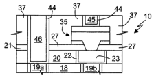
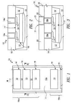
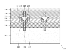
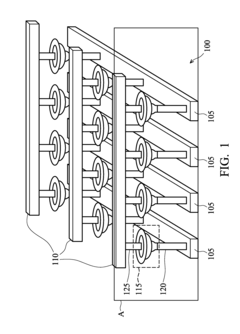
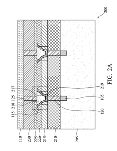
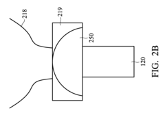
Process for manufacturing a phase change memory array in Cu-damascene technology and phase change memory array manufactured thereby
PatentInactiveUS7259040B2
Innovation
- The Cu-damascene technology is employed to simplify the etching process by substituting AlCu with copper lines, which are formed after shaping the resistive bit lines, and using a dual Damascene technique to improve thermal budget and precision, thereby overcoming the compatibility issues and increasing yield.
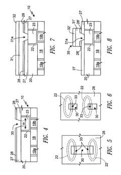
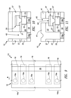
Phase change memory cell
PatentActiveUS20120104339A1
Innovation
- A simplified manufacturing method for phase change random access memory (PCRAM) cells using a single mask to create a crown structure, reducing costs and complexity, and employing a chemical-mechanical polishing (CMP) process to form phase change and electrode regions, allowing for easy adaptation of upper contacts.
Supply Chain Resilience for PCM Materials
The global supply chain for Phase Change Memory (PCM) materials faces significant vulnerabilities due to the concentration of critical raw materials in specific geographic regions. Germanium, antimony, and tellurium—key elements in PCM production—are predominantly sourced from China, creating potential bottlenecks during geopolitical tensions. Recent disruptions during the COVID-19 pandemic highlighted these vulnerabilities when manufacturing facilities in Asia experienced prolonged shutdowns, causing delays in PCM component availability for global technology manufacturers.
To address these challenges, leading semiconductor companies are implementing multi-sourcing strategies for critical PCM materials. Intel and Micron have established relationships with suppliers across different regions, including North America, Europe, and Southeast Asia, to reduce dependency on single-source materials. Samsung has invested in vertical integration by acquiring stakes in mining operations to secure direct access to raw materials, particularly tellurium and germanium compounds.
Material substitution research represents another promising approach to supply chain resilience. IBM Research and academic institutions are exploring alternative compositions that reduce reliance on scarce elements while maintaining performance characteristics. Early results indicate that selenium-based compounds may partially replace tellurium in certain PCM applications, potentially alleviating supply constraints for this critical element.
Recycling and circular economy initiatives are gaining traction as sustainable solutions. Advanced recycling technologies can recover up to 85% of germanium and tellurium from end-of-life electronic devices. Companies like TSMC have implemented closed-loop manufacturing systems that recapture and reuse materials during production processes, reducing raw material requirements by approximately 30%.
Inventory management strategies have evolved in response to recent disruptions. Major PCM manufacturers now maintain strategic reserves of critical materials sufficient for 6-9 months of production, compared to the previous industry standard of 2-3 months. This approach, while increasing carrying costs, provides significant protection against short-term supply disruptions.
Collaborative industry initiatives are emerging to address systemic supply chain vulnerabilities. The Semiconductor Supply Chain Consortium, comprising major PCM manufacturers, material suppliers, and technology companies, is developing industry standards for material certification and establishing shared early warning systems for potential supply disruptions. These collaborative efforts aim to increase transparency throughout the supply chain and enable more coordinated responses to emerging challenges.
Environmental Impact of PCM Manufacturing
The manufacturing of Phase Change Memory (PCM) technology carries significant environmental implications that warrant careful consideration as the industry advances toward smaller technology nodes. PCM production processes involve several environmentally sensitive materials and energy-intensive manufacturing steps that contribute to its overall ecological footprint.
The fabrication of PCM devices requires rare earth elements and heavy metals such as germanium, antimony, and tellurium. As technology nodes shrink, the extraction and processing of these materials become increasingly resource-intensive, leading to habitat disruption, soil degradation, and water pollution in mining regions. The projected increase in PCM adoption across computing platforms will likely intensify demand for these limited resources, potentially exacerbating environmental stress in extraction zones.
Energy consumption represents another critical environmental factor in PCM manufacturing. While smaller technology nodes theoretically improve energy efficiency per bit, the transition to advanced nodes demands more sophisticated fabrication equipment and cleanroom facilities with higher energy requirements. Current estimates suggest that a typical PCM fabrication facility consumes between 30-50 megawatt-hours per day, with projections indicating a 15-20% increase in energy demand for each technology node advancement.
Water usage in PCM manufacturing presents additional environmental challenges. The production process requires ultra-pure water for cleaning and cooling, with a single fabrication facility consuming millions of gallons annually. As nodes shrink to 10nm and below, the water purification requirements become more stringent, increasing both water consumption and the energy needed for purification processes.
Chemical waste management constitutes a significant environmental concern in PCM production. The etching and deposition processes utilize various hazardous chemicals including strong acids, solvents, and specialized gases. Advanced technology nodes require more precise chemical processes, often resulting in increased waste generation per wafer despite the smaller feature sizes. Industry data indicates that chemical waste treatment costs have risen approximately 22% for each technology node advancement over the past decade.
Carbon emissions associated with PCM manufacturing stem primarily from energy consumption and chemical processes. While manufacturers are implementing carbon reduction initiatives, the complex requirements of smaller technology nodes often offset efficiency gains. Current industry estimates suggest that PCM production generates 30-45 kg of CO2 equivalent per wafer, with projections showing only modest reductions of 5-8% per technology node despite significant sustainability investments.
Unlock deeper insights with Patsnap Eureka Quick Research — get a full tech report to explore trends and direct your research. Try now!
Generate Your Research Report Instantly with AI Agent
Supercharge your innovation with Patsnap Eureka AI Agent Platform!