

Nickel Molybdenum Alloy Pellets: Comprehensive Analysis Of Composition, Processing, And Industrial Applications
JUL 16, 20259 MIN READ
Generate Your Research Report Instantly with AI Agent
PatSnap Eureka helps you evaluate technical feasibility & market potential.
Chiplet Evolution and Objectives
Chiplet technology has emerged as a revolutionary approach in multicore processor design, offering a paradigm shift in how complex integrated circuits are developed and manufactured. The evolution of chiplets can be traced back to the early 2010s when the semiconductor industry began facing significant challenges in scaling monolithic chip designs. As Moore's Law started to slow down, chiplets presented a viable solution to continue improving processor performance and efficiency.
The primary objective of chiplet technology is to overcome the limitations of traditional monolithic chip designs by disaggregating complex systems into smaller, more manageable components. This approach aims to enhance yield, reduce costs, and improve overall system performance. By allowing different functional blocks to be manufactured separately and then integrated onto a single package, chiplets enable the use of optimal process nodes for each component, leading to better power efficiency and performance characteristics.
The evolution of chiplet technology has been marked by several key milestones. Initially, the focus was on developing reliable interconnect technologies to enable high-bandwidth, low-latency communication between chiplets. This led to the development of advanced packaging technologies such as silicon interposers and through-silicon vias (TSVs). As the technology matured, industry standards like Universal Chiplet Interconnect Express (UCIe) emerged, promoting interoperability and accelerating adoption across the semiconductor ecosystem.
Another significant objective of chiplet technology is to enable more flexible and scalable processor designs. By leveraging a modular approach, manufacturers can mix and match different chiplets to create a wide range of products tailored to specific market segments. This flexibility allows for faster time-to-market and more cost-effective product development cycles, as companies can reuse existing chiplet designs across multiple product lines.
The evolution of chiplets has also been driven by the increasing demand for specialized computing solutions, particularly in areas such as artificial intelligence, high-performance computing, and edge computing. Chiplet technology enables the integration of diverse components, such as CPUs, GPUs, memory, and custom accelerators, into a single package, facilitating the development of highly optimized systems for specific workloads.
Looking ahead, the objectives for chiplet technology include further miniaturization of interconnects, improved thermal management techniques, and enhanced integration methodologies. Researchers and industry leaders are also exploring advanced 3D integration techniques, which promise to unlock even greater performance and efficiency gains. As the technology continues to evolve, it is expected to play a crucial role in shaping the future of multicore processor design, enabling more powerful, efficient, and versatile computing systems across a wide range of applications.
The primary objective of chiplet technology is to overcome the limitations of traditional monolithic chip designs by disaggregating complex systems into smaller, more manageable components. This approach aims to enhance yield, reduce costs, and improve overall system performance. By allowing different functional blocks to be manufactured separately and then integrated onto a single package, chiplets enable the use of optimal process nodes for each component, leading to better power efficiency and performance characteristics.
The evolution of chiplet technology has been marked by several key milestones. Initially, the focus was on developing reliable interconnect technologies to enable high-bandwidth, low-latency communication between chiplets. This led to the development of advanced packaging technologies such as silicon interposers and through-silicon vias (TSVs). As the technology matured, industry standards like Universal Chiplet Interconnect Express (UCIe) emerged, promoting interoperability and accelerating adoption across the semiconductor ecosystem.
Another significant objective of chiplet technology is to enable more flexible and scalable processor designs. By leveraging a modular approach, manufacturers can mix and match different chiplets to create a wide range of products tailored to specific market segments. This flexibility allows for faster time-to-market and more cost-effective product development cycles, as companies can reuse existing chiplet designs across multiple product lines.
The evolution of chiplets has also been driven by the increasing demand for specialized computing solutions, particularly in areas such as artificial intelligence, high-performance computing, and edge computing. Chiplet technology enables the integration of diverse components, such as CPUs, GPUs, memory, and custom accelerators, into a single package, facilitating the development of highly optimized systems for specific workloads.
Looking ahead, the objectives for chiplet technology include further miniaturization of interconnects, improved thermal management techniques, and enhanced integration methodologies. Researchers and industry leaders are also exploring advanced 3D integration techniques, which promise to unlock even greater performance and efficiency gains. As the technology continues to evolve, it is expected to play a crucial role in shaping the future of multicore processor design, enabling more powerful, efficient, and versatile computing systems across a wide range of applications.
Market Demand Analysis
The market demand for chiplet-based multicore processor designs has been steadily increasing in recent years, driven by the growing need for more powerful and efficient computing solutions across various industries. As traditional monolithic chip designs approach their physical limits, chiplet technology offers a promising alternative to meet the escalating performance requirements while managing power consumption and manufacturing costs.
In the data center and cloud computing sector, the demand for chiplet-based processors is particularly strong. Major cloud service providers and enterprise customers are seeking high-performance, scalable solutions to handle the exponential growth in data processing and artificial intelligence workloads. Chiplet technology allows for the integration of specialized processing units, such as AI accelerators, alongside general-purpose cores, providing a flexible and customizable platform for diverse computing needs.
The telecommunications industry is another significant driver of chiplet demand, especially with the ongoing rollout of 5G networks and the anticipated transition to 6G in the coming years. Network equipment manufacturers require processors that can handle increased data throughput and complex signal processing tasks while maintaining energy efficiency. Chiplet-based designs offer the ability to combine high-performance cores with specialized networking components, meeting the unique requirements of this sector.
In the consumer electronics market, there is a growing interest in chiplet technology for next-generation devices. Smartphone manufacturers are exploring chiplet-based solutions to enhance performance and energy efficiency in mobile processors. Similarly, the gaming industry is looking towards chiplet designs to push the boundaries of graphics processing and overall system performance in consoles and high-end PCs.
The automotive sector represents an emerging market for chiplet-based processors, driven by the increasing computerization of vehicles and the development of autonomous driving technologies. Advanced driver assistance systems (ADAS) and infotainment systems require powerful, energy-efficient processors that can be tailored to specific automotive requirements. Chiplet technology offers the flexibility to integrate various functionalities while meeting stringent reliability and safety standards.
Industrial automation and the Internet of Things (IoT) are also contributing to the demand for chiplet-based solutions. These applications often require a combination of high-performance processing, low power consumption, and the ability to integrate specialized sensors or communication modules. Chiplet technology provides a modular approach that can be adapted to diverse industrial and IoT use cases.
The market potential for chiplet-based multicore processors is substantial, with industry analysts projecting significant growth in the coming years. As more companies invest in research and development of chiplet technologies, we can expect to see increased adoption across various sectors, driving innovation and competition in the semiconductor industry.
In the data center and cloud computing sector, the demand for chiplet-based processors is particularly strong. Major cloud service providers and enterprise customers are seeking high-performance, scalable solutions to handle the exponential growth in data processing and artificial intelligence workloads. Chiplet technology allows for the integration of specialized processing units, such as AI accelerators, alongside general-purpose cores, providing a flexible and customizable platform for diverse computing needs.
The telecommunications industry is another significant driver of chiplet demand, especially with the ongoing rollout of 5G networks and the anticipated transition to 6G in the coming years. Network equipment manufacturers require processors that can handle increased data throughput and complex signal processing tasks while maintaining energy efficiency. Chiplet-based designs offer the ability to combine high-performance cores with specialized networking components, meeting the unique requirements of this sector.
In the consumer electronics market, there is a growing interest in chiplet technology for next-generation devices. Smartphone manufacturers are exploring chiplet-based solutions to enhance performance and energy efficiency in mobile processors. Similarly, the gaming industry is looking towards chiplet designs to push the boundaries of graphics processing and overall system performance in consoles and high-end PCs.
The automotive sector represents an emerging market for chiplet-based processors, driven by the increasing computerization of vehicles and the development of autonomous driving technologies. Advanced driver assistance systems (ADAS) and infotainment systems require powerful, energy-efficient processors that can be tailored to specific automotive requirements. Chiplet technology offers the flexibility to integrate various functionalities while meeting stringent reliability and safety standards.
Industrial automation and the Internet of Things (IoT) are also contributing to the demand for chiplet-based solutions. These applications often require a combination of high-performance processing, low power consumption, and the ability to integrate specialized sensors or communication modules. Chiplet technology provides a modular approach that can be adapted to diverse industrial and IoT use cases.
The market potential for chiplet-based multicore processors is substantial, with industry analysts projecting significant growth in the coming years. As more companies invest in research and development of chiplet technologies, we can expect to see increased adoption across various sectors, driving innovation and competition in the semiconductor industry.
Chiplet Tech Challenges
The development of chiplet technology for multicore processor design faces several significant challenges that need to be addressed for widespread adoption and optimal performance. One of the primary obstacles is the interconnect technology between chiplets. As the number of chiplets increases, the complexity of inter-chiplet communication grows exponentially, requiring advanced packaging and interconnect solutions to maintain high bandwidth and low latency.
Power management and thermal dissipation present another major hurdle. With multiple chiplets in close proximity, managing heat distribution and power consumption becomes increasingly complex. Efficient power delivery networks and advanced cooling solutions are essential to prevent thermal bottlenecks and ensure consistent performance across all chiplets.
Standardization of chiplet interfaces and protocols is a critical challenge that impacts interoperability and market adoption. The lack of universal standards for chiplet-to-chiplet communication and integration hinders the development of a robust ecosystem and limits the potential for mix-and-match chiplet designs from different vendors.
Design and verification complexity increases significantly with chiplet-based architectures. Engineers must contend with new challenges in system-level integration, timing closure, and signal integrity across chiplet boundaries. This complexity extends to the software domain, where optimizing operating systems and applications for chiplet-based processors requires new approaches to resource allocation and task scheduling.
Manufacturing and yield management present unique challenges in chiplet production. While chiplets allow for better yield management by isolating defects to smaller die areas, the assembly process introduces new potential points of failure. Ensuring consistent quality and performance across multiple chiplets requires advanced testing and validation methodologies.
Cost considerations remain a significant factor in chiplet adoption. While chiplets offer potential cost savings through better yield management and the ability to mix and match different process nodes, the initial investment in new design tools, manufacturing processes, and packaging technologies can be substantial.
Lastly, security and data integrity in multi-chiplet systems pose new challenges. Protecting sensitive data as it moves between chiplets and ensuring the authenticity of individual chiplets in a system are critical concerns that require innovative security measures and protocols.
Addressing these challenges will be crucial for the continued advancement and widespread adoption of chiplet technology in multicore processor design. As the industry works towards solutions, we can expect to see significant innovations in packaging, interconnect technologies, design methodologies, and standardization efforts.
Power management and thermal dissipation present another major hurdle. With multiple chiplets in close proximity, managing heat distribution and power consumption becomes increasingly complex. Efficient power delivery networks and advanced cooling solutions are essential to prevent thermal bottlenecks and ensure consistent performance across all chiplets.
Standardization of chiplet interfaces and protocols is a critical challenge that impacts interoperability and market adoption. The lack of universal standards for chiplet-to-chiplet communication and integration hinders the development of a robust ecosystem and limits the potential for mix-and-match chiplet designs from different vendors.
Design and verification complexity increases significantly with chiplet-based architectures. Engineers must contend with new challenges in system-level integration, timing closure, and signal integrity across chiplet boundaries. This complexity extends to the software domain, where optimizing operating systems and applications for chiplet-based processors requires new approaches to resource allocation and task scheduling.
Manufacturing and yield management present unique challenges in chiplet production. While chiplets allow for better yield management by isolating defects to smaller die areas, the assembly process introduces new potential points of failure. Ensuring consistent quality and performance across multiple chiplets requires advanced testing and validation methodologies.
Cost considerations remain a significant factor in chiplet adoption. While chiplets offer potential cost savings through better yield management and the ability to mix and match different process nodes, the initial investment in new design tools, manufacturing processes, and packaging technologies can be substantial.
Lastly, security and data integrity in multi-chiplet systems pose new challenges. Protecting sensitive data as it moves between chiplets and ensuring the authenticity of individual chiplets in a system are critical concerns that require innovative security measures and protocols.
Addressing these challenges will be crucial for the continued advancement and widespread adoption of chiplet technology in multicore processor design. As the industry works towards solutions, we can expect to see significant innovations in packaging, interconnect technologies, design methodologies, and standardization efforts.
Current Chiplet Solutions
01 Modular chiplet architecture
Chiplet techniques involve designing integrated circuits as smaller, modular components that can be combined on a single package. This approach allows for more flexible and efficient designs, enabling the integration of different functionalities and technologies. The modular nature of chiplets streamlines the design process by allowing reuse of pre-validated components and easier customization for specific applications.- Modular chiplet architecture: Chiplet techniques involve designing integrated circuits as modular components that can be combined on a single package. This approach allows for more flexible and efficient design, enabling the integration of different functionalities and technologies. The modular nature of chiplets streamlines the design process by allowing reuse of pre-validated components and easier customization for specific applications.
- Interconnect optimization for chiplets: Efficient interconnect design is crucial for chiplet-based systems. This involves optimizing the communication pathways between different chiplets and within the package. Advanced interconnect technologies, such as silicon interposers or advanced packaging techniques, are employed to ensure high-speed, low-latency communication between chiplets, contributing to overall system performance and power efficiency.
- Power management in chiplet designs: Effective power management is essential in chiplet-based systems to optimize performance and energy efficiency. This includes implementing sophisticated power gating techniques, voltage scaling, and thermal management strategies across multiple chiplets. Advanced power management techniques help in reducing overall power consumption and improving the energy efficiency of the system.
- Design automation for chiplet integration: Automated design tools and methodologies are crucial for streamlining the chiplet integration process. These tools assist in various aspects of chiplet-based system design, including floor planning, signal integrity analysis, thermal analysis, and overall system optimization. Advanced EDA (Electronic Design Automation) tools specifically tailored for chiplet designs help in reducing design time and improving overall system performance.
- Testing and validation strategies for chiplets: Developing effective testing and validation strategies is crucial for ensuring the reliability and performance of chiplet-based systems. This includes pre-integration testing of individual chiplets, as well as comprehensive system-level testing after integration. Advanced testing methodologies, such as built-in self-test (BIST) and design-for-test (DFT) techniques, are adapted for chiplet architectures to streamline the validation process and ensure high-quality, reliable products.
02 Advanced packaging technologies
Chiplet-based designs rely on advanced packaging technologies to integrate multiple dies efficiently. These technologies include 2.5D and 3D packaging, interposers, and through-silicon vias (TSVs). Such packaging methods enable high-bandwidth connections between chiplets, reducing latency and power consumption while improving overall system performance.Expand Specific Solutions03 Design automation and optimization
Streamlined chiplet design processes leverage advanced EDA (Electronic Design Automation) tools and methodologies. These tools assist in optimizing chiplet placement, interconnect routing, and power distribution. AI-driven design automation techniques are increasingly used to explore vast design spaces efficiently, leading to more optimal chiplet configurations and faster time-to-market.Expand Specific Solutions04 Standardization and interoperability
To facilitate widespread adoption of chiplet technologies, industry efforts are focused on developing standards for chiplet interfaces and protocols. These standards aim to ensure interoperability between chiplets from different vendors, enabling a more diverse and competitive ecosystem. Standardization efforts also contribute to streamlining the design process by providing common frameworks and reference designs.Expand Specific Solutions05 Power and thermal management
Efficient power and thermal management are crucial aspects of chiplet-based designs. Techniques such as dynamic voltage and frequency scaling, power gating, and advanced cooling solutions are employed to optimize energy efficiency and manage heat dissipation across multiple chiplets. These strategies are essential for maintaining performance and reliability in complex chiplet configurations.Expand Specific Solutions
Key Chiplet Players
The research on Chiplet techniques for streamlined multicore processor design is currently in a dynamic phase, with significant market potential and growing technological maturity. The industry is transitioning from traditional monolithic designs to more modular and scalable chiplet-based architectures. Major players like Intel, AMD, and Qualcomm are actively investing in this technology, recognizing its potential to address scaling challenges and improve performance. The market size is expanding rapidly, driven by increasing demand for high-performance computing in data centers, AI, and edge computing applications. While the technology is maturing, there is still room for innovation and optimization, particularly in areas such as interconnect technologies and system integration.
Intel Corp.
Technical Solution: Intel's chiplet approach, known as "Foveros," utilizes 3D packaging technology to stack multiple chiplets vertically. This allows for the integration of diverse IP blocks and process nodes within a single package. Intel's Meteor Lake processors employ this technology, combining compute, graphics, and AI tiles[1]. The company has also introduced its Universal Chiplet Interconnect Express (UCIe) standard, which aims to create an open ecosystem for chiplet-based designs[2]. Intel's implementation includes advanced features such as through-silicon vias (TSVs) and micro-bumps for high-bandwidth, low-latency inter-chiplet communication[3].
Strengths: Vertical integration capabilities, advanced packaging technologies, and industry-standard initiatives. Weaknesses: Potential thermal challenges in 3D stacking and higher manufacturing complexity.
Advanced Micro Devices, Inc.
Technical Solution: AMD's chiplet strategy revolves around its "Infinity Fabric" interconnect technology, which allows for modular chip design. The company's Zen architecture utilizes multiple chiplets, known as Core Complex Dies (CCDs), connected to an I/O die[4]. This approach enables AMD to mix and match different process nodes for various components, optimizing performance and cost. AMD has implemented this technology in both its EPYC server processors and Ryzen desktop CPUs, achieving high core counts and improved yields[5]. The company has also been exploring 3D V-Cache technology, stacking additional cache memory on top of the processor die to enhance performance[6].
Strengths: Scalability, flexibility in chip design, and improved yields. Weaknesses: Potential latency issues between chiplets and complexity in thermal management.
Core Chiplet Innovations
Method of executing programmable atomic unit resources within a multi-process system
PatentActiveUS12020062B2
Innovation
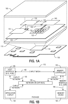
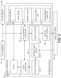
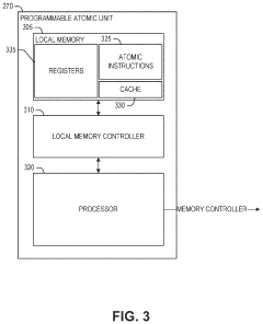
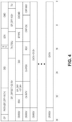
- A method is disclosed that involves determining a unique identifier for a programmable atomic transaction within a process, using a mapping table to generate a system-wide identifier, and issuing requests to a memory controller to perform the transaction, allowing for efficient execution and response handling through a programmable atomic unit.
Continual flow processor pipeline
PatentInactiveUS20060090061A1
Innovation
- The system identifies instructions dependent on long-latency operations, moves them to a slice data buffer, and re-introduces them into the pipeline when the long-latency operations are completed, allowing scheduler and register resources to be reclaimed for other instructions, thus maintaining a non-blocking processor pipeline flow.


Chiplet Integration Strategies
Chiplet integration strategies have emerged as a crucial aspect of modern multicore processor design, offering a pathway to overcome the limitations of monolithic chip manufacturing. These strategies involve the assembly of multiple smaller dies, or chiplets, onto a single package, enabling the creation of more complex and powerful processors while mitigating the challenges associated with large-scale chip production.
One of the primary integration strategies is the use of advanced packaging technologies, such as 2.5D and 3D integration. In 2.5D integration, chiplets are placed side by side on an interposer, which provides high-density interconnects between the dies. This approach allows for the combination of chiplets manufactured using different process nodes, optimizing performance and cost. 3D integration takes this concept further by stacking chiplets vertically, significantly reducing the overall footprint and improving communication speeds between components.
Another key strategy is the development of standardized interfaces for chiplet communication. Industry initiatives like the Universal Chiplet Interconnect Express (UCIe) aim to establish common protocols and physical interfaces, facilitating interoperability between chiplets from different manufacturers. This standardization is crucial for creating a more diverse and competitive chiplet ecosystem, potentially reducing costs and accelerating innovation in processor design.
Power delivery and thermal management are critical considerations in chiplet integration. Strategies to address these challenges include the use of through-silicon vias (TSVs) for efficient power distribution in 3D stacked configurations and the implementation of advanced cooling solutions such as integrated liquid cooling or microfluidic channels within the package.
The design of the interconnect fabric between chiplets is another vital aspect of integration. High-bandwidth, low-latency connections are essential for maintaining performance as the number of chiplets increases. Optical interconnects are being explored as a potential solution, offering the possibility of higher data rates and lower power consumption compared to traditional electrical interconnects.
Yield management is a significant factor in chiplet integration strategies. By dividing a large chip design into smaller chiplets, manufacturers can improve overall yield rates, as defects in one chiplet do not necessitate discarding the entire processor. This approach also allows for more flexible binning and product differentiation, enabling companies to create a wider range of products from a single chiplet design.
In conclusion, chiplet integration strategies are revolutionizing multicore processor design, offering increased flexibility, improved performance, and potentially lower costs. As these techniques continue to evolve, they are likely to play an increasingly important role in shaping the future of computing hardware.
One of the primary integration strategies is the use of advanced packaging technologies, such as 2.5D and 3D integration. In 2.5D integration, chiplets are placed side by side on an interposer, which provides high-density interconnects between the dies. This approach allows for the combination of chiplets manufactured using different process nodes, optimizing performance and cost. 3D integration takes this concept further by stacking chiplets vertically, significantly reducing the overall footprint and improving communication speeds between components.
Another key strategy is the development of standardized interfaces for chiplet communication. Industry initiatives like the Universal Chiplet Interconnect Express (UCIe) aim to establish common protocols and physical interfaces, facilitating interoperability between chiplets from different manufacturers. This standardization is crucial for creating a more diverse and competitive chiplet ecosystem, potentially reducing costs and accelerating innovation in processor design.
Power delivery and thermal management are critical considerations in chiplet integration. Strategies to address these challenges include the use of through-silicon vias (TSVs) for efficient power distribution in 3D stacked configurations and the implementation of advanced cooling solutions such as integrated liquid cooling or microfluidic channels within the package.
The design of the interconnect fabric between chiplets is another vital aspect of integration. High-bandwidth, low-latency connections are essential for maintaining performance as the number of chiplets increases. Optical interconnects are being explored as a potential solution, offering the possibility of higher data rates and lower power consumption compared to traditional electrical interconnects.
Yield management is a significant factor in chiplet integration strategies. By dividing a large chip design into smaller chiplets, manufacturers can improve overall yield rates, as defects in one chiplet do not necessitate discarding the entire processor. This approach also allows for more flexible binning and product differentiation, enabling companies to create a wider range of products from a single chiplet design.
In conclusion, chiplet integration strategies are revolutionizing multicore processor design, offering increased flexibility, improved performance, and potentially lower costs. As these techniques continue to evolve, they are likely to play an increasingly important role in shaping the future of computing hardware.
Chiplet Ecosystem Development
The chiplet ecosystem has rapidly evolved in recent years, driven by the need for more efficient and scalable multicore processor designs. This ecosystem encompasses a wide range of technologies, standards, and industry collaborations that enable the development and integration of chiplets into complex systems-on-chip (SoCs).
At the core of the chiplet ecosystem are advanced packaging technologies, such as 2.5D and 3D integration, which allow for the interconnection of multiple chiplets within a single package. These technologies have been crucial in overcoming the limitations of traditional monolithic chip designs, enabling higher performance, improved power efficiency, and greater design flexibility.
Standardization efforts have played a significant role in fostering the growth of the chiplet ecosystem. Industry consortia, such as the Open Compute Project (OCP) and the CHIPS Alliance, have been instrumental in developing open standards for chiplet interfaces and interconnects. These standards, including the Advanced Interface Bus (AIB) and Universal Chiplet Interconnect Express (UCIe), have facilitated interoperability between chiplets from different vendors and accelerated the adoption of chiplet-based designs.
The chiplet ecosystem has also seen the emergence of specialized intellectual property (IP) providers focused on developing reusable chiplet designs and integration solutions. These companies offer a range of pre-validated chiplets, from high-performance CPU and GPU cores to specialized accelerators for AI and machine learning applications. This has lowered the barrier to entry for companies looking to leverage chiplet technology in their products.
Manufacturing and testing infrastructure have evolved to support the unique requirements of chiplet-based designs. Advanced foundries have invested in new processes and equipment to enable high-density interconnects and fine-pitch bumping required for chiplet integration. Similarly, test and validation methodologies have been adapted to address the challenges of testing individual chiplets and ensuring system-level functionality.
The chiplet ecosystem has fostered new business models and collaborations within the semiconductor industry. Fabless companies can now focus on their core competencies while leveraging chiplets from other providers to create differentiated products. This has led to increased specialization and innovation across the industry, with companies developing expertise in specific areas such as high-speed SerDes, memory interfaces, or power management chiplets.
As the chiplet ecosystem continues to mature, it is driving innovation in areas such as heterogeneous computing, disaggregated server architectures, and edge computing solutions. The flexibility and scalability offered by chiplet-based designs are enabling new approaches to system architecture that can better address the diverse and evolving needs of modern computing applications.
At the core of the chiplet ecosystem are advanced packaging technologies, such as 2.5D and 3D integration, which allow for the interconnection of multiple chiplets within a single package. These technologies have been crucial in overcoming the limitations of traditional monolithic chip designs, enabling higher performance, improved power efficiency, and greater design flexibility.
Standardization efforts have played a significant role in fostering the growth of the chiplet ecosystem. Industry consortia, such as the Open Compute Project (OCP) and the CHIPS Alliance, have been instrumental in developing open standards for chiplet interfaces and interconnects. These standards, including the Advanced Interface Bus (AIB) and Universal Chiplet Interconnect Express (UCIe), have facilitated interoperability between chiplets from different vendors and accelerated the adoption of chiplet-based designs.
The chiplet ecosystem has also seen the emergence of specialized intellectual property (IP) providers focused on developing reusable chiplet designs and integration solutions. These companies offer a range of pre-validated chiplets, from high-performance CPU and GPU cores to specialized accelerators for AI and machine learning applications. This has lowered the barrier to entry for companies looking to leverage chiplet technology in their products.
Manufacturing and testing infrastructure have evolved to support the unique requirements of chiplet-based designs. Advanced foundries have invested in new processes and equipment to enable high-density interconnects and fine-pitch bumping required for chiplet integration. Similarly, test and validation methodologies have been adapted to address the challenges of testing individual chiplets and ensuring system-level functionality.
The chiplet ecosystem has fostered new business models and collaborations within the semiconductor industry. Fabless companies can now focus on their core competencies while leveraging chiplets from other providers to create differentiated products. This has led to increased specialization and innovation across the industry, with companies developing expertise in specific areas such as high-speed SerDes, memory interfaces, or power management chiplets.
As the chiplet ecosystem continues to mature, it is driving innovation in areas such as heterogeneous computing, disaggregated server architectures, and edge computing solutions. The flexibility and scalability offered by chiplet-based designs are enabling new approaches to system architecture that can better address the diverse and evolving needs of modern computing applications.
Unlock deeper insights with PatSnap Eureka Quick Research — get a full tech report to explore trends and direct your research. Try now!
Generate Your Research Report Instantly with AI Agent
Supercharge your innovation with PatSnap Eureka AI Agent Platform!