Electroless Nickel Coatings for Electronic Components
OCT 23, 202510 MIN READ
Generate Your Research Report Instantly with AI Agent
Patsnap Eureka helps you evaluate technical feasibility & market potential.
Electroless Nickel Coating Technology Background and Objectives
Electroless nickel plating technology has evolved significantly since its inception in the early 20th century, with major advancements occurring post-World War II. Initially developed as an alternative to electrolytic plating processes, this chemical deposition method has become increasingly vital in the electronics industry due to its ability to create uniform coatings on complex geometries without requiring electrical current.
The evolution of electroless nickel coating technology has been driven by the miniaturization trend in electronic components, which demands higher precision, reliability, and performance from protective coatings. From early phosphorus-based formulations to modern composite coatings incorporating particles like PTFE, silicon carbide, or diamond, the technology has continuously adapted to meet increasingly stringent industry requirements.
Current technological trajectories show a clear movement toward environmentally friendly formulations that eliminate hazardous substances like lead, cadmium, and certain phosphorus compounds. This shift aligns with global regulatory frameworks such as RoHS and REACH, which have significantly influenced coating chemistry development in recent decades.
The primary objective of electroless nickel coating research for electronic components centers on enhancing performance characteristics while addressing environmental concerns. Key performance targets include superior corrosion resistance in harsh environments, improved wear resistance for components subject to mechanical stress, and optimized electrical properties—particularly controlled conductivity and solderability.
Another critical goal involves improving coating uniformity and adhesion on increasingly complex substrate materials used in modern electronics, including various metal alloys, ceramics, and certain polymers. The industry seeks coatings that maintain integrity across wide temperature ranges, from cryogenic conditions to the elevated temperatures experienced during soldering operations and device operation.
Process efficiency represents another significant objective, with research focused on developing formulations that offer faster deposition rates while maintaining quality, extended bath life to reduce waste, and lower energy consumption during the plating process. These improvements directly impact manufacturing costs and environmental footprint.
The integration of nanotechnology into electroless nickel plating presents perhaps the most promising frontier, with research exploring nano-structured coatings that could revolutionize performance characteristics. These advanced materials aim to provide unprecedented combinations of hardness, wear resistance, and corrosion protection while maintaining excellent electrical properties required for electronic applications.
Market Demand Analysis for Electronic Component Surface Treatments
The global market for electronic component surface treatments has experienced significant growth in recent years, driven by the expanding electronics industry and increasing demand for high-performance components. The electroless nickel coating segment specifically has shown robust growth due to its superior properties and versatility in electronic applications. Current market estimates value the global electroless plating market at approximately 2 billion USD, with a compound annual growth rate of 6-7% projected through 2028.
Electronic component manufacturers are increasingly seeking surface treatment solutions that can meet multiple performance requirements simultaneously. The primary market drivers include miniaturization trends in electronics, growing complexity of electronic devices, and increasing reliability requirements in harsh operating environments. Electroless nickel coatings address these needs by providing excellent corrosion resistance, uniform deposition on complex geometries, and good solderability - critical factors for modern electronic components.
The automotive electronics sector represents one of the fastest-growing application areas, particularly with the rise of electric vehicles requiring more sophisticated electronic control systems. Consumer electronics continues to be the largest market segment, with smartphones, tablets, and wearable devices demanding components with enhanced durability and performance characteristics. The aerospace and defense sectors also present significant opportunities, as these industries require components with exceptional reliability under extreme conditions.
Regional analysis reveals Asia-Pacific as the dominant market for electronic component surface treatments, accounting for over 45% of global demand. This concentration aligns with the region's position as the manufacturing hub for electronics. North America and Europe follow as significant markets, with particular emphasis on high-value applications in medical electronics, aerospace, and industrial automation.
Customer requirements are evolving toward more environmentally sustainable solutions, creating market pressure for nickel coating processes with reduced environmental impact. Regulations limiting the use of certain chemicals in manufacturing processes, particularly in Europe and North America, are reshaping market dynamics and driving innovation in greener coating technologies.
Price sensitivity varies significantly by application segment, with consumer electronics manufacturers typically more cost-conscious than aerospace or medical device producers. However, across all segments, there is growing recognition of the total cost benefits of high-quality surface treatments that extend component lifespan and improve reliability, potentially offsetting higher initial treatment costs.
The market shows clear segmentation between standard coating services and specialized high-performance solutions, with the latter commanding premium pricing but growing at a faster rate due to the increasing complexity of electronic applications.
Current Status and Technical Challenges in Electroless Nickel Plating
Electroless nickel plating technology has evolved significantly over the past decades, establishing itself as a critical surface treatment method for electronic components. Currently, the global market for electroless nickel coatings is experiencing steady growth, with an estimated market value of approximately $1.8 billion in 2023 and projected to reach $2.5 billion by 2028, representing a CAGR of 6.8%. This growth is primarily driven by increasing demands from the electronics, automotive, and aerospace industries.
The current state of electroless nickel plating technology demonstrates considerable maturity in several aspects. Medium-phosphorus nickel coatings (6-9% P) remain the most widely adopted solution for electronic components due to their balanced properties of corrosion resistance and hardness. High-phosphorus variants (>10% P) have gained traction for applications requiring superior corrosion protection, while low-phosphorus formulations (<6% P) are preferred when maximum hardness and wear resistance are essential.
Despite its widespread adoption, electroless nickel plating faces significant technical challenges. Bath stability remains a persistent issue, with plating solutions typically having limited lifespans of 4-8 metal turnovers before requiring replacement. This instability stems from the accumulation of orthophosphites and other by-products that gradually degrade plating performance and increase the risk of spontaneous decomposition.
Environmental concerns present another major challenge, as traditional electroless nickel formulations contain hazardous substances such as lead compounds, cadmium, and formaldehyde. Regulatory frameworks worldwide, including RoHS in Europe and similar initiatives in Asia and North America, are increasingly restricting these substances, necessitating the development of environmentally friendly alternatives.
Adhesion issues between nickel coatings and various substrate materials continue to challenge manufacturers, particularly with newer composite materials and advanced polymers used in modern electronic components. Inconsistent coating thickness distribution on complex geometries remains problematic, with variations often exceeding ±10% on intricate parts, compromising performance reliability.
Geographically, Asia-Pacific dominates the electroless nickel plating market, accounting for approximately 45% of global capacity, with China alone representing nearly 25%. North America and Europe follow with approximately 30% and 20% market share respectively. Recent years have witnessed significant technological advancements in Japan and South Korea, particularly in the development of nano-composite electroless nickel coatings incorporating ceramic particles for enhanced performance characteristics.
The miniaturization trend in electronics has introduced new challenges, as plating uniformity becomes increasingly critical at micro and nano scales. Traditional electroless nickel processes struggle to maintain consistent deposit properties within the tight tolerances required for advanced semiconductor packaging and microelectromechanical systems (MEMS).
Current Technical Solutions for Electronic Component Coating
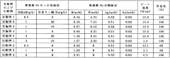
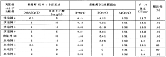
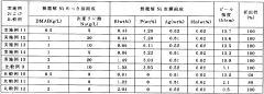
01 Composition and formulation of electroless nickel plating baths
Electroless nickel plating baths typically contain nickel salts, reducing agents, complexing agents, stabilizers, and pH adjusters. The composition can be optimized to achieve specific coating properties such as hardness, corrosion resistance, and uniformity. Various formulations may include hypophosphite-based systems, borohydride-based systems, or specialized additives to enhance deposition rate and coating quality.- Composition and formulation of electroless nickel plating baths: Electroless nickel plating baths typically contain nickel salts, reducing agents, complexing agents, stabilizers, and pH adjusters. The composition can be optimized to control the deposition rate, coating properties, and stability of the bath. Various formulations may include hypophosphite-based systems, borohydride-based systems, or other reducing agents to facilitate the autocatalytic deposition of nickel without the need for external electrical current.
- Incorporation of additives and co-deposited elements: Additives and co-deposited elements can be incorporated into electroless nickel coatings to enhance specific properties. Phosphorus, boron, and various metals such as tungsten, molybdenum, or cobalt can be co-deposited to improve hardness, wear resistance, corrosion resistance, and thermal stability. The concentration of these elements can be controlled to achieve desired coating characteristics for specific applications.
- Post-treatment and heat treatment processes: Post-treatment processes, particularly heat treatment, can significantly enhance the properties of electroless nickel coatings. Heat treatment at various temperatures can transform the amorphous structure of as-deposited coatings into crystalline structures, increasing hardness and wear resistance. Other post-treatments may include passivation, sealing, or application of topcoats to further improve corrosion resistance and other functional properties.
- Substrate preparation and pretreatment methods: Proper substrate preparation is crucial for achieving high-quality electroless nickel coatings with good adhesion. Pretreatment processes may include cleaning, degreasing, etching, and activation steps. For non-catalytic surfaces, activation with palladium or other catalysts may be necessary to initiate the electroless deposition process. The pretreatment methods vary depending on the substrate material and the intended application of the coating.
- Specialized applications and composite coatings: Electroless nickel coatings can be tailored for specialized applications such as electronics, automotive components, aerospace parts, and chemical processing equipment. Composite coatings incorporating particles such as silicon carbide, diamond, or PTFE can be created to enhance specific properties like wear resistance, lubricity, or hydrophobicity. These specialized coatings often require modified bath compositions and deposition parameters to achieve the desired functionality.
02 Surface preparation and pretreatment methods
Proper surface preparation is critical for successful electroless nickel coating adhesion. Pretreatment processes may include cleaning, degreasing, etching, and activation steps. Specialized pretreatment methods can be employed for different substrate materials such as metals, plastics, and ceramics to ensure optimal coating adhesion and performance.Expand Specific Solutions03 Nickel-phosphorus and nickel-boron coating properties
Electroless nickel coatings can be classified based on their phosphorus or boron content, which significantly affects their properties. Low, medium, and high phosphorus coatings offer different characteristics in terms of hardness, corrosion resistance, magnetic properties, and wear resistance. Nickel-boron coatings typically provide superior hardness and wear resistance compared to nickel-phosphorus coatings.Expand Specific Solutions04 Post-treatment and heat treatment processes
Post-deposition treatments such as heat treatment can significantly enhance the properties of electroless nickel coatings. Heat treatment at specific temperatures can increase hardness, wear resistance, and adhesion strength. Other post-treatments may include passivation, sealing, or application of topcoats to further improve corrosion resistance and functional properties of the coating.Expand Specific Solutions05 Advanced applications and composite coatings
Electroless nickel coatings can be modified with particles or other materials to create composite coatings with enhanced properties. These include nickel-phosphorus-particle composites incorporating materials such as silicon carbide, diamond, or PTFE for improved wear resistance, lubricity, or specialized functions. Advanced applications include electronics, aerospace, automotive, and chemical processing industries where specific coating properties are required.Expand Specific Solutions
Key Industry Players in Electroless Nickel Coating Market
The electroless nickel coating market for electronic components is currently in a growth phase, with increasing demand driven by miniaturization trends in electronics and automotive applications. The global market size is estimated to reach several billion dollars by 2025, expanding at a CAGR of 4-6%. Technologically, the field shows moderate maturity with ongoing innovations in coating formulations. Leading players include Japan Pure Chemical Co., specializing in noble metal plating chemicals; BYD Co., focusing on battery applications; Texas Instruments and Murata Manufacturing, implementing advanced coating technologies for semiconductor components; and research institutions like the Institute of Metal Research CAS driving fundamental innovations. Chinese manufacturers such as Konfoong Materials and Huaxun Semiconductor are rapidly advancing their capabilities, particularly in specialized electronic applications.
Japan Pure Chemical Co., Ltd.
Technical Solution: Japan Pure Chemical Co., Ltd. has developed advanced electroless nickel plating solutions specifically designed for electronic components. Their proprietary EN-PLATE NI series features precisely controlled phosphorus content (ranging from 2-14%) to meet various electronic application requirements. The company has pioneered environmentally compliant formulations that are free from lead, cadmium, and other restricted substances, making them RoHS and REACH compliant. Their technology incorporates specialized additives that enhance deposit uniformity on complex geometries common in modern electronic components. Japan Pure Chemical's solutions deliver exceptional corrosion resistance (>1000 hours in salt spray testing) and maintain stable electrical properties across varying environmental conditions. Their process optimization allows for controlled deposition rates (15-25 μm/hour) while maintaining excellent adhesion to various substrate materials including copper, aluminum, and ceramics commonly used in electronic applications.
Strengths: Superior deposit uniformity on complex geometries; excellent environmental compliance; exceptional corrosion resistance with stable electrical properties. Weaknesses: Higher cost compared to conventional solutions; requires more precise process control parameters; may have longer processing times for specialized high-performance coatings.
Institute of Metal Research Chinese Academy of Sciences
Technical Solution: The Institute of Metal Research (IMR) at the Chinese Academy of Sciences has developed innovative electroless nickel coating technologies specifically engineered for electronic component applications. Their research has yielded advanced Ni-P-X composite coatings (where X represents nano-additives like SiC, Al2O3, or graphene) that significantly enhance wear resistance and electrical performance. IMR's proprietary process achieves ultra-thin (2-5 μm) uniform deposits with exceptional adhesion strength (>30 MPa) on various substrates. Their technology incorporates precise control of phosphorus content (1-12%) to tailor specific properties for different electronic applications. The institute has pioneered low-temperature deposition methods (60-75°C) that minimize thermal stress on sensitive electronic components while maintaining excellent coating quality. Their electroless nickel solutions also feature self-regulating deposition mechanisms that ensure consistent thickness even on complex geometries with recessed areas common in modern electronic packages.
Strengths: Advanced composite coating capabilities with nano-additives; precise phosphorus content control for tailored properties; excellent uniformity on complex geometries. Weaknesses: Some formulations may require specialized equipment for optimal results; higher implementation costs compared to standard processes; certain nano-enhanced coatings may have limited commercial scalability.
Core Patents and Innovations in Electroless Nickel Deposition
Electroless nickel plating coat and pretreatment method for forming the electroless nickel plating coat
PatentActiveJP2021080513A
Innovation
- An electroless nickel plating film and pretreatment method using boron, phosphorus, and silver or copper catalysts, eliminating the need for palladium, with specific compositions and conditions to ensure good film properties.

Environmental Impact and Sustainability Considerations
The environmental impact of electroless nickel plating processes has become a critical consideration in the electronics industry. Traditional electroless nickel baths contain several chemicals that pose significant environmental concerns, including nickel salts, which are classified as carcinogenic, and reducing agents like sodium hypophosphite that contribute to water pollution. The disposal of spent plating solutions represents a major environmental challenge, as these solutions contain heavy metals that can contaminate soil and water systems if not properly treated.
Recent regulatory frameworks, such as the European Union's Restriction of Hazardous Substances (RoHS) and Registration, Evaluation, Authorization and Restriction of Chemicals (REACH), have placed increasing pressure on manufacturers to adopt more environmentally friendly plating processes. These regulations have accelerated research into green alternatives and sustainable practices within the electroless nickel coating industry.
Significant progress has been made in developing more sustainable electroless nickel plating solutions. Low-phosphorus nickel formulations have emerged as environmentally preferable options, as they typically require fewer chemical additives and generate less hazardous waste. Additionally, closed-loop recycling systems have been implemented in advanced manufacturing facilities, allowing for the recovery and reuse of nickel from spent plating baths, thereby reducing raw material consumption and waste generation.
Water consumption represents another environmental concern in electroless nickel plating operations. The process traditionally requires multiple rinsing stages, consuming substantial volumes of water. Innovative approaches such as cascade rinsing systems and advanced filtration technologies have demonstrated water usage reductions of up to 60% in some facilities, significantly improving the sustainability profile of these operations.
Energy efficiency improvements have also contributed to reducing the environmental footprint of electroless nickel plating. Traditional processes operate at elevated temperatures (85-95°C), consuming considerable energy. Recent technological advancements have enabled lower-temperature plating processes that maintain coating quality while reducing energy requirements by approximately 25-30%.
Life cycle assessment (LCA) studies comparing electroless nickel coatings with alternative surface finishing technologies have revealed interesting sustainability trade-offs. While the plating process itself has environmental impacts, the extended service life and enhanced performance of nickel-coated components often result in net environmental benefits through reduced replacement frequency and improved energy efficiency in end applications.
Looking forward, the industry is exploring bio-based reducing agents and catalysts to replace conventional chemicals in electroless nickel baths. Preliminary research indicates that plant-derived compounds may offer viable alternatives to traditional reducing agents, potentially transforming electroless nickel plating into a more environmentally benign process aligned with circular economy principles.
Quality Control and Reliability Testing Methods
Quality control and reliability testing are critical aspects of electroless nickel coating processes for electronic components, ensuring consistent performance and longevity in demanding applications. The industry has established comprehensive testing methodologies that evaluate both physical properties and functional performance of these coatings.
Surface inspection techniques form the foundation of quality control, with optical microscopy and scanning electron microscopy (SEM) being widely employed to detect surface defects such as pits, cracks, and nodules. Advanced imaging technologies like 3D profilometry provide quantitative data on surface roughness and coating uniformity, essential parameters for components requiring precise dimensional tolerances.
Thickness measurement represents another crucial quality parameter, typically assessed through X-ray fluorescence (XRF), cross-sectional microscopy, or coulometric methods. For electronic applications, coating thickness uniformity is particularly important as variations can affect electrical properties and component reliability. Industry standards generally require thickness variations to remain within ±10% across critical surfaces.
Adhesion testing methods, including tape tests (ASTM D3359) and scratch tests, evaluate the coating's bonding strength to the substrate. Poor adhesion can lead to delamination during thermal cycling or mechanical stress, causing catastrophic failure in electronic assemblies. More sophisticated bend and impact tests simulate real-world mechanical stresses that components might experience during assembly or operation.
Corrosion resistance testing, essential for evaluating long-term reliability, includes salt spray exposure (ASTM B117), humidity testing, and electrochemical impedance spectroscopy (EIS). These accelerated aging tests provide predictive data on coating performance under harsh environmental conditions. For electronic applications, specialized tests evaluating resistance to flux residues and cleaning chemicals are also conducted.
Electrical property verification includes measurements of contact resistance, solderability, and dielectric strength. These parameters directly impact the component's functional performance in electronic circuits. Thermal cycling tests (-65°C to +150°C) assess coating integrity under temperature fluctuations, while thermal shock tests evaluate resistance to rapid temperature changes that electronic components frequently encounter.
Wear resistance testing using pin-on-disk tribometers or Taber abraders quantifies the coating's durability against mechanical abrasion, particularly important for connectors and other components subject to repeated mating cycles. Hardness measurements, typically performed using microhardness testers, provide additional data on mechanical properties.
Statistical process control (SPC) methodologies are increasingly implemented to monitor these quality parameters continuously, enabling early detection of process drift and maintaining consistent coating quality. Advanced manufacturers employ automated inspection systems integrated with machine learning algorithms to detect subtle defect patterns that might escape conventional testing methods.
Unlock deeper insights with Patsnap Eureka Quick Research — get a full tech report to explore trends and direct your research. Try now!
Generate Your Research Report Instantly with AI Agent
Supercharge your innovation with Patsnap Eureka AI Agent Platform!