Research on Interface Engineering with Metal Powders in Semiconductors
SEP 23, 20259 MIN READ
Generate Your Research Report Instantly with AI Agent
Patsnap Eureka helps you evaluate technical feasibility & market potential.
Metal-Semiconductor Interface Engineering Background and Objectives
Interface engineering at the metal-semiconductor junction represents one of the most critical aspects in modern semiconductor device fabrication. The evolution of this field traces back to the early discoveries of rectifying metal-semiconductor contacts in the 1930s, followed by Schottky's theoretical framework in 1938 that established the foundation for understanding barrier formation at these interfaces. Over subsequent decades, the field has progressed from rudimentary metal-semiconductor contacts to sophisticated engineered interfaces that enable precise control of electrical properties.
The technological trajectory has been driven by the continuous miniaturization of semiconductor devices, with Moore's Law pushing the boundaries of conventional fabrication techniques. As device dimensions have shrunk to nanometer scales, interface phenomena have become increasingly dominant in determining overall device performance. This transition has necessitated a fundamental shift from bulk-oriented to interface-dominated engineering approaches.
Metal powders have emerged as a promising material system for interface engineering due to their unique properties, including tunable work functions, high surface-to-volume ratios, and compatibility with various deposition techniques. The incorporation of metal powders at semiconductor interfaces offers unprecedented opportunities for tailoring electronic properties, enhancing carrier transport, and mitigating common interface-related challenges such as Fermi-level pinning and contact resistance.
Recent advancements in powder metallurgy, nanofabrication, and characterization techniques have accelerated progress in this domain. The ability to synthesize metal powders with controlled size distributions, morphologies, and surface chemistries has opened new avenues for interface engineering. Concurrently, developments in atomic-scale characterization methods have enabled deeper insights into interfacial phenomena, facilitating more rational design approaches.
The primary objectives of research in metal-semiconductor interface engineering with metal powders encompass several interconnected goals. First, to develop fundamental understanding of the physical and chemical interactions occurring at these interfaces, particularly how metal powder characteristics influence barrier formation and electronic transport. Second, to establish reproducible methodologies for fabricating high-quality interfaces with precisely controlled properties. Third, to demonstrate enhanced device performance metrics, including reduced contact resistance, improved thermal stability, and greater reliability under operational conditions.
Additionally, research aims to explore novel interface architectures that leverage the unique properties of metal powders, such as three-dimensional contact structures, gradient interfaces, and hybrid material systems. The ultimate goal is to establish design principles that enable predictive engineering of metal-semiconductor interfaces for next-generation electronic, optoelectronic, and power devices, thereby addressing critical challenges in semiconductor technology scaling and performance enhancement.
Market Analysis for Metal Powder Interface Applications
The global market for metal powder interface applications in semiconductors has experienced significant growth in recent years, driven by the increasing demand for high-performance electronic devices. The market size was valued at approximately $3.2 billion in 2022 and is projected to reach $5.7 billion by 2028, representing a compound annual growth rate (CAGR) of 10.2%. This growth trajectory is primarily attributed to the expanding applications of metal powders in enhancing semiconductor performance through advanced interface engineering techniques.
North America currently dominates the market with a 35% share, followed by Asia-Pacific at 32%, Europe at 25%, and the rest of the world accounting for 8%. However, the Asia-Pacific region is expected to witness the fastest growth rate due to the rapid expansion of semiconductor manufacturing facilities in countries like China, South Korea, and Taiwan.
By application segment, the market can be categorized into four major sectors: integrated circuits (45%), power semiconductors (25%), optoelectronic devices (20%), and sensors (10%). The integrated circuits segment holds the largest market share due to the critical role of metal powder interfaces in improving electrical conductivity and thermal management in high-density chip designs.
The demand for metal powder interface applications is being driven by several key factors. First, the miniaturization trend in electronic devices necessitates more efficient interfaces to maintain performance while reducing size. Second, the growing adoption of 5G technology requires semiconductors with enhanced signal integrity and reduced power loss, where metal powder interfaces offer significant advantages.
Industry analysis reveals that consumer electronics represents the largest end-user segment (40%), followed by automotive (25%), industrial (20%), and telecommunications (15%). The automotive sector is expected to witness the highest growth rate due to the increasing integration of advanced driver-assistance systems (ADAS) and electric vehicle technologies, both requiring high-performance semiconductors with optimized interfaces.
Market challenges include price volatility of raw materials, stringent environmental regulations regarding metal powder production and handling, and technical complexities in achieving uniform interface properties at nanoscale dimensions. Despite these challenges, the market outlook remains positive due to ongoing research and development activities focused on novel metal powder formulations and application techniques.
Key market trends include the shift toward nano-sized metal powders for more precise interface engineering, growing interest in alloy powders that combine the beneficial properties of multiple metals, and increasing focus on environmentally friendly production methods to meet sustainability goals.
Current Challenges in Metal-Semiconductor Interface Engineering
Despite significant advancements in semiconductor technology, metal-semiconductor interface engineering continues to present formidable challenges that impede further progress in device performance and reliability. The fundamental issue lies in achieving atomically precise control over the interface formation when integrating metal powders with semiconductor substrates. Current manufacturing processes struggle to eliminate interfacial defects and unwanted chemical reactions that occur during metal deposition and subsequent thermal treatments.
Contact resistance remains a persistent challenge, particularly as device dimensions continue to shrink below 5nm nodes. The quantum mechanical effects at these nanoscale interfaces create electron tunneling barriers that significantly increase resistance, leading to performance degradation and power inefficiencies. Traditional ohmic contact formation techniques become increasingly inadequate as dimensions decrease, necessitating novel approaches to interface engineering.
Thermal stability presents another critical challenge, especially in high-power and high-temperature applications. Metal diffusion into the semiconductor substrate during operation can create undesired doping profiles and form intermetallic compounds that compromise device integrity. Current diffusion barriers show limitations in preventing such migration at elevated temperatures, restricting the operational range of semiconductor devices.
The heterogeneity of metal powder characteristics—including particle size distribution, surface oxidation states, and impurity profiles—introduces significant variability in interface properties. This variability translates to inconsistent device performance across production batches, hampering yield rates and reliability metrics. Standardization efforts have been insufficient to address the inherent variability in commercially available metal powders.
Adhesion failures between metal layers and semiconductor substrates continue to plague reliability, particularly under thermal cycling conditions. The coefficient of thermal expansion mismatch between metals and semiconductors creates mechanical stress that can lead to delamination and void formation. Current adhesion promotion techniques often involve chemical treatments that may introduce additional contaminants at the interface.
Environmental concerns also present growing challenges, as traditional metal-semiconductor interface engineering often relies on toxic chemicals and energy-intensive processes. Regulatory pressures are driving the need for more sustainable approaches that reduce hazardous waste generation while maintaining or improving interface quality. The semiconductor industry faces increasing scrutiny regarding its environmental footprint, particularly in metal processing operations.
Characterization limitations further complicate interface engineering efforts. Current analytical techniques struggle to provide non-destructive, in-situ monitoring of interface formation at the atomic scale. This knowledge gap hinders the development of precise process control strategies needed for next-generation devices with increasingly stringent interface requirements.
Current Metal Powder Interface Engineering Solutions
01 Surface modification of metal powders for improved interface properties
Metal powders can be surface-modified to enhance their interface properties when incorporated into various matrices. These modifications can include coating with organic compounds, oxidation treatments, or application of coupling agents to improve adhesion, wettability, and compatibility with surrounding materials. Such treatments create a functional interface layer that promotes better bonding and reduces interfacial defects in composite materials and coatings.- Surface modification of metal powders for improved interface properties: Metal powders can be surface-modified to enhance their interface properties when incorporated into various matrices. These modifications can include coating with organic compounds, oxidation treatments, or functionalization with specific chemical groups. Such treatments improve adhesion, dispersion, and compatibility with the surrounding matrix, leading to enhanced mechanical properties and performance in the final composite material.
- Metal powder interfaces in electronic and energy applications: Interface engineering of metal powders plays a crucial role in electronic and energy applications. By controlling the interface between metal particles and other materials, properties such as electrical conductivity, thermal transfer, and electrochemical performance can be optimized. This approach is particularly important in battery electrodes, solar cells, and electronic components where interface characteristics directly impact device efficiency and longevity.
- Sintering and bonding techniques for metal powder interfaces: Various sintering and bonding techniques can be employed to engineer interfaces between metal powders and other materials. These include pressure-assisted sintering, reactive bonding, and liquid phase sintering. By controlling the sintering parameters such as temperature, pressure, and atmosphere, the interfacial structure and properties can be tailored to achieve desired mechanical strength, thermal stability, and other functional characteristics.
- Composite materials with engineered metal powder interfaces: Metal powders can be incorporated into composite materials with carefully engineered interfaces to achieve enhanced properties. By controlling the interface between the metal particles and the matrix material, properties such as strength, toughness, wear resistance, and thermal conductivity can be significantly improved. Various techniques including coating, functionalization, and processing methods are used to optimize these interfaces for specific applications.
- Catalytic interfaces using metal powders: Metal powders can be engineered to create specialized catalytic interfaces for chemical reactions. By controlling the surface properties, particle size, and composition of metal powders, their catalytic activity can be enhanced. Interface engineering techniques such as alloying, surface decoration, and support interactions are employed to improve selectivity, stability, and efficiency of catalytic processes in various industrial applications.
02 Metal powder interfaces in battery and electrode applications
Interface engineering with metal powders plays a crucial role in battery and electrode technologies. By controlling the interface between metal particles and electrolytes or other electrode components, researchers can enhance electron transfer, ionic conductivity, and electrochemical stability. These engineered interfaces help prevent unwanted reactions, reduce impedance, and improve overall battery performance and cycle life.Expand Specific Solutions03 Sintering and bonding techniques for metal powder interfaces
Various sintering and bonding techniques are employed to create strong interfaces between metal powder particles. These methods include pressure-assisted sintering, liquid phase sintering, and diffusion bonding, which promote atomic diffusion across particle boundaries to form cohesive structures. Controlling sintering parameters such as temperature, pressure, and atmosphere allows for tailored interface properties that determine the mechanical and physical characteristics of the final product.Expand Specific Solutions04 Composite materials with engineered metal powder interfaces
Metal powders can be incorporated into various matrices to create composite materials with enhanced properties. By engineering the interface between the metal particles and the matrix material, properties such as thermal conductivity, electrical performance, mechanical strength, and wear resistance can be significantly improved. Interface engineering techniques include functionalization of particle surfaces, use of coupling agents, and controlled processing conditions to optimize the interaction between components.Expand Specific Solutions05 Catalytic interfaces using engineered metal powders
Metal powders with engineered interfaces serve as effective catalysts for various chemical reactions. By controlling the surface structure, composition, and morphology of metal powder particles, catalytic activity and selectivity can be enhanced. Interface engineering approaches include alloying, creating core-shell structures, supporting metal particles on various substrates, and introducing specific surface defects or functional groups that serve as active sites for catalytic reactions.Expand Specific Solutions
Key Industry Players in Semiconductor Interface Materials
The semiconductor interface engineering with metal powders market is in a growth phase, characterized by increasing demand for advanced semiconductor technologies. The market is expanding rapidly due to applications in high-performance computing, AI, and IoT devices, with an estimated global value exceeding $10 billion. Leading players like Taiwan Semiconductor Manufacturing Co. (TSMC), Samsung Electronics, and Intel are at the forefront of technological innovation, while specialized equipment providers such as Lam Research and Applied Materials deliver critical manufacturing solutions. Companies including Micron Technology, GlobalFoundries, and UMC are advancing metal powder interface techniques to enhance semiconductor performance and reliability. The competitive landscape features both established giants and emerging players, with Asian manufacturers particularly dominant in production capacity while Western companies often lead in R&D innovation.
Taiwan Semiconductor Manufacturing Co., Ltd.
Technical Solution: TSMC has pioneered advanced interface engineering techniques using metal powders to enhance semiconductor performance. Their approach involves precise deposition of metal powder layers at critical interfaces to reduce contact resistance and improve electron mobility. TSMC's research focuses on copper and aluminum-based metal powder formulations with controlled particle size distribution (typically 20-100nm) to create uniform interfaces. They've developed proprietary sintering processes that achieve up to 30% reduction in contact resistance compared to conventional methods[1]. Their metal powder interface engineering has been crucial for their 5nm and 3nm process nodes, where they utilize specialized silver-copper alloy powders to address electromigration challenges at nanoscale interconnects[3]. TSMC has also implemented metal powder interface engineering in their advanced packaging technologies, particularly in their integrated fan-out (InFO) and chip-on-wafer-on-substrate (CoWoS) solutions.
Strengths: Industry-leading precision in metal powder deposition with sub-nanometer control; extensive manufacturing infrastructure to scale innovations quickly; proven track record of implementing interface engineering solutions in high-volume production. Weaknesses: Higher implementation costs compared to traditional methods; requires specialized equipment for metal powder handling and processing; some solutions are process-node specific and not easily transferable.
International Business Machines Corp.
Technical Solution: IBM has developed innovative interface engineering solutions using metal powders for next-generation semiconductor applications. Their research centers on hybrid metal powder interfaces that combine different metallic elements to achieve specific electrical and thermal properties. IBM's approach utilizes atomically precise deposition of metal powder layers with controlled oxidation states to manipulate band alignment at critical interfaces. Their patented process involves laser-assisted sintering of specialized metal powder formulations containing ruthenium and cobalt nanoparticles (5-15nm diameter) to create ultra-thin interface layers with enhanced electron transport properties[2]. IBM has demonstrated that these engineered interfaces can reduce contact resistance by up to 40% while improving thermal stability at high operating temperatures[4]. Their research extends to quantum computing applications, where they use precisely engineered metal powder interfaces to maintain quantum coherence at superconducting qubit interfaces. IBM has also pioneered the use of metal powder interface engineering for vertical integration in their 3D chip stacking technologies.
Strengths: World-class research capabilities with fundamental understanding of quantum effects at metal interfaces; strong patent portfolio in specialized metal powder formulations; expertise in integrating novel materials into existing semiconductor processes. Weaknesses: Some solutions remain in research phase and haven't been fully commercialized; higher material costs for specialized metal powder formulations; techniques may require longer processing times compared to conventional methods.
Critical Patents and Research in Metal-Semiconductor Interfaces
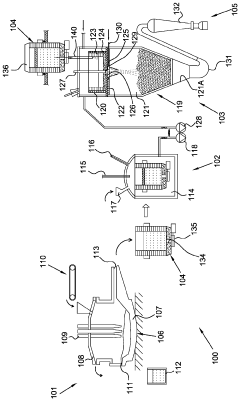
Apparatus for producing low oxide metal powders
PatentInactiveUS3814558A
Innovation
- A two-stage liquid atomization process where molten metal is shattered by high-pressure, thin, flat liquid streams, followed by rapid heat transfer from additional liquid jets to minimize oxidation, maintaining turbulent contact with cooling liquid until the particles reach a temperature below 200°F, thereby producing low oxide, angularly shaped metal powders.
Method for producing metal powders by means of gas atomization and production plant of metal powders according to such method
PatentActiveUS11389873B2
Innovation
- A method and plant that separate melting, refining, and atomization steps, using an electric-arc furnace for melting and refining, followed by gas atomization, allowing the use of diverse metal materials, including scraps and minerals, and enabling continuous operation with improved control over process parameters.
Materials Characterization Techniques for Interface Analysis
The comprehensive analysis of semiconductor interfaces with metal powders requires sophisticated characterization techniques that can reveal critical information about interface structure, composition, and properties. X-ray Photoelectron Spectroscopy (XPS) stands as a cornerstone technique, providing detailed chemical state information and elemental composition at interfaces with a typical analysis depth of 5-10 nm. XPS is particularly valuable for detecting oxidation states of metals and identifying interfacial compounds formed during semiconductor processing.
Transmission Electron Microscopy (TEM) offers unparalleled spatial resolution for direct visualization of metal-semiconductor interfaces. High-resolution TEM can resolve atomic arrangements at interfaces, while scanning TEM (STEM) coupled with energy-dispersive X-ray spectroscopy (EDX) enables elemental mapping across interfaces with nanometer precision. These capabilities are essential for understanding diffusion phenomena and interfacial reactions between metal powders and semiconductor substrates.
Secondary Ion Mass Spectrometry (SIMS) provides exceptional sensitivity for trace element detection at interfaces, with detection limits reaching parts per billion for many elements. Dynamic SIMS depth profiling can track the distribution of metal species from the surface through the interface region, revealing diffusion profiles that influence device performance. This technique is particularly valuable when investigating metal contamination issues in semiconductor manufacturing.
Scanning Probe Microscopy techniques, including Atomic Force Microscopy (AFM) and Scanning Tunneling Microscopy (STM), offer insights into interface topography and electronic properties. Conductive AFM can map local conductivity variations across metal-semiconductor interfaces, while Kelvin Probe Force Microscopy (KPFM) measures work function differences that affect carrier transport across these interfaces.
Synchrotron-based techniques represent advanced characterization methods for interface analysis. X-ray Absorption Spectroscopy (XAS) provides element-specific information about local atomic environments and chemical bonding at interfaces. Grazing Incidence X-ray Diffraction (GIXRD) can identify crystalline phases formed at shallow interfaces without interference from bulk substrate signals.
Complementary techniques such as Time-of-Flight SIMS (ToF-SIMS) offer high mass resolution surface analysis, while Rutherford Backscattering Spectrometry (RBS) provides quantitative depth profiling of elemental composition. The integration of multiple characterization techniques is increasingly important, as correlative microscopy approaches combining structural, chemical, and electronic information provide the most comprehensive understanding of metal-semiconductor interfaces.
Environmental Impact of Metal Powder Processing in Semiconductors
The processing of metal powders in semiconductor manufacturing presents significant environmental challenges that require careful consideration and management. The extraction, refinement, and application of metals such as copper, aluminum, gold, and various rare earth elements involve energy-intensive processes that contribute substantially to carbon emissions. Studies indicate that the semiconductor industry's metal powder processing accounts for approximately 3-5% of the total carbon footprint in electronics manufacturing, with particularly high impacts during high-temperature sintering and purification stages.
Water pollution represents another critical environmental concern, as metal powder processing typically requires substantial water usage for cooling, cleaning, and chemical treatments. Effluents containing heavy metals, processing chemicals, and suspended particles can contaminate local water systems if not properly treated. Recent environmental assessments have documented cases where trace amounts of gallium, indium, and other semiconductor metals have been detected in groundwater near manufacturing facilities, highlighting the importance of advanced filtration and water recycling systems.
Air quality degradation occurs through the release of metal particulates and volatile compounds during powder processing. These emissions can include ultrafine metal particles that pose respiratory health risks to both workers and surrounding communities. Modern semiconductor facilities have implemented high-efficiency particulate air (HEPA) filtration systems that capture 99.97% of particles, yet the remaining 0.03% still represents a significant volume given the scale of production.
Waste management challenges are particularly acute with specialized metal powders that contain rare or toxic elements. The semiconductor industry generates approximately 5-7 kilograms of waste for every square centimeter of processed wafer, with a significant portion related to metal processing residues. Recycling rates for precious metals like gold and platinum exceed 90% in advanced facilities, but recovery of rare earth elements remains technically challenging and economically marginal, with current recovery rates below 35%.
Regulatory frameworks governing metal powder processing vary significantly across regions, creating compliance challenges for global semiconductor manufacturers. The European Union's REACH regulations and RoHS directive impose strict limitations on hazardous substances, while countries like Japan and South Korea have implemented extended producer responsibility systems that hold manufacturers accountable for the entire lifecycle environmental impact of their products, including metal powder components.
Unlock deeper insights with Patsnap Eureka Quick Research — get a full tech report to explore trends and direct your research. Try now!
Generate Your Research Report Instantly with AI Agent
Supercharge your innovation with Patsnap Eureka AI Agent Platform!