

Study on Silicon Carbide Wafer Thickness Parameters
OCT 14, 20259 MIN READ
Generate Your Research Report Instantly with AI Agent
PatSnap Eureka helps you evaluate technical feasibility & market potential.
SiC Wafer Technology Background and Objectives
Silicon Carbide (SiC) has emerged as a revolutionary semiconductor material in the power electronics industry over the past three decades. Initially discovered in 1824 by Jöns Jacob Berzelius, SiC remained primarily an industrial abrasive until the late 20th century when its exceptional semiconductor properties began to be exploited. The evolution of SiC wafer technology has been marked by continuous improvements in crystal growth techniques, from the primitive Acheson process to the sophisticated modified Lely method and now the dominant Physical Vapor Transport (PVT) process.
The fundamental advantage of SiC lies in its wide bandgap (3.2 eV for 4H-SiC), which is approximately three times that of silicon (1.1 eV). This property, combined with high thermal conductivity (3-4 times that of silicon) and high breakdown electric field strength (10 times that of silicon), makes SiC an ideal candidate for high-power, high-temperature, and high-frequency applications where traditional silicon-based devices reach their physical limitations.
Wafer thickness represents a critical parameter in SiC technology development, directly influencing device performance, manufacturing yield, and cost-effectiveness. Historically, SiC wafers were significantly thicker (500-600 μm) than their silicon counterparts due to the challenges in material processing. The industry has been progressively moving toward thinner wafers to optimize electrical performance and reduce material costs, while balancing mechanical stability requirements.
The technical objectives of this study on SiC wafer thickness parameters are multifaceted. First, we aim to establish the optimal thickness range for different SiC device applications, considering the trade-offs between electrical performance, thermal management, and mechanical robustness. Second, we seek to identify the relationship between wafer thickness and key manufacturing challenges such as wafer bow, warp, and surface roughness. Third, we intend to explore innovative thinning techniques that can maintain crystal quality while reducing thickness.
Current industry trends indicate a push toward 150mm and 200mm diameter SiC wafers with controlled thickness parameters to support high-volume manufacturing. The standardization of these parameters is crucial for the broader adoption of SiC technology across automotive, industrial, and renewable energy sectors. Leading manufacturers are targeting thickness reductions to 350-400 μm for standard applications, with specialized ultra-thin wafers (below 200 μm) being developed for specific high-performance applications.
The evolution trajectory suggests that wafer thickness optimization will continue to be a key differentiator in SiC technology advancement, with significant implications for device performance, manufacturing economics, and market competitiveness. This study aims to provide a comprehensive framework for understanding and optimizing this critical parameter in the context of rapidly evolving SiC semiconductor technology.
The fundamental advantage of SiC lies in its wide bandgap (3.2 eV for 4H-SiC), which is approximately three times that of silicon (1.1 eV). This property, combined with high thermal conductivity (3-4 times that of silicon) and high breakdown electric field strength (10 times that of silicon), makes SiC an ideal candidate for high-power, high-temperature, and high-frequency applications where traditional silicon-based devices reach their physical limitations.
Wafer thickness represents a critical parameter in SiC technology development, directly influencing device performance, manufacturing yield, and cost-effectiveness. Historically, SiC wafers were significantly thicker (500-600 μm) than their silicon counterparts due to the challenges in material processing. The industry has been progressively moving toward thinner wafers to optimize electrical performance and reduce material costs, while balancing mechanical stability requirements.
The technical objectives of this study on SiC wafer thickness parameters are multifaceted. First, we aim to establish the optimal thickness range for different SiC device applications, considering the trade-offs between electrical performance, thermal management, and mechanical robustness. Second, we seek to identify the relationship between wafer thickness and key manufacturing challenges such as wafer bow, warp, and surface roughness. Third, we intend to explore innovative thinning techniques that can maintain crystal quality while reducing thickness.
Current industry trends indicate a push toward 150mm and 200mm diameter SiC wafers with controlled thickness parameters to support high-volume manufacturing. The standardization of these parameters is crucial for the broader adoption of SiC technology across automotive, industrial, and renewable energy sectors. Leading manufacturers are targeting thickness reductions to 350-400 μm for standard applications, with specialized ultra-thin wafers (below 200 μm) being developed for specific high-performance applications.
The evolution trajectory suggests that wafer thickness optimization will continue to be a key differentiator in SiC technology advancement, with significant implications for device performance, manufacturing economics, and market competitiveness. This study aims to provide a comprehensive framework for understanding and optimizing this critical parameter in the context of rapidly evolving SiC semiconductor technology.
Market Demand Analysis for Thin SiC Wafers
The global market for thin Silicon Carbide (SiC) wafers has been experiencing robust growth, driven primarily by the increasing demand for high-performance power electronics in electric vehicles, renewable energy systems, and industrial applications. Current market assessments indicate that the SiC power semiconductor market is expanding at a compound annual growth rate of approximately 30% and is projected to reach $3 billion by 2025, with thin wafers representing a significant portion of this growth.
The automotive sector stands as the primary demand driver for thin SiC wafers, particularly for electric vehicle (EV) applications. As automotive manufacturers worldwide accelerate their transition to electric powertrains, the need for more efficient power conversion systems has intensified. Thin SiC wafers enable the production of devices that can operate at higher temperatures, voltages, and frequencies while maintaining smaller form factors and improved thermal management characteristics.
Power electronics manufacturers are increasingly specifying thinner SiC wafers to optimize device performance and reduce material costs. The industry is witnessing a gradual transition from traditional 350-500 μm wafers toward ultra-thin wafers in the 100-200 μm range. This shift is particularly evident in applications requiring enhanced thermal dissipation and reduced on-resistance, such as traction inverters for EVs and high-frequency switching devices.
Regional market analysis reveals that Asia-Pacific currently dominates the demand landscape, with China, Japan, and South Korea leading in consumption. Europe follows closely, driven by its robust automotive manufacturing base and aggressive carbon reduction policies. North America represents another significant market, particularly as domestic semiconductor manufacturing initiatives gain momentum.
Supply chain considerations are becoming increasingly critical in the thin SiC wafer market. The limited number of suppliers capable of producing high-quality thin SiC wafers has created potential bottlenecks as demand continues to surge. Major semiconductor manufacturers are responding by establishing strategic partnerships with SiC wafer suppliers or developing in-house capabilities to secure their supply chains.
Price sensitivity analysis indicates that while thin SiC wafers command premium pricing compared to silicon alternatives, the performance benefits and overall system cost reductions they enable are driving continued adoption. Industry forecasts suggest that economies of scale and manufacturing improvements will gradually reduce the cost differential, further accelerating market penetration.
Emerging applications in 5G infrastructure, aerospace systems, and grid-scale power conversion are expected to create additional demand vectors for thin SiC wafers. These applications value the reduced switching losses, higher power density, and improved reliability that thin SiC-based devices offer, particularly in harsh operating environments or where system efficiency is paramount.
The automotive sector stands as the primary demand driver for thin SiC wafers, particularly for electric vehicle (EV) applications. As automotive manufacturers worldwide accelerate their transition to electric powertrains, the need for more efficient power conversion systems has intensified. Thin SiC wafers enable the production of devices that can operate at higher temperatures, voltages, and frequencies while maintaining smaller form factors and improved thermal management characteristics.
Power electronics manufacturers are increasingly specifying thinner SiC wafers to optimize device performance and reduce material costs. The industry is witnessing a gradual transition from traditional 350-500 μm wafers toward ultra-thin wafers in the 100-200 μm range. This shift is particularly evident in applications requiring enhanced thermal dissipation and reduced on-resistance, such as traction inverters for EVs and high-frequency switching devices.
Regional market analysis reveals that Asia-Pacific currently dominates the demand landscape, with China, Japan, and South Korea leading in consumption. Europe follows closely, driven by its robust automotive manufacturing base and aggressive carbon reduction policies. North America represents another significant market, particularly as domestic semiconductor manufacturing initiatives gain momentum.
Supply chain considerations are becoming increasingly critical in the thin SiC wafer market. The limited number of suppliers capable of producing high-quality thin SiC wafers has created potential bottlenecks as demand continues to surge. Major semiconductor manufacturers are responding by establishing strategic partnerships with SiC wafer suppliers or developing in-house capabilities to secure their supply chains.
Price sensitivity analysis indicates that while thin SiC wafers command premium pricing compared to silicon alternatives, the performance benefits and overall system cost reductions they enable are driving continued adoption. Industry forecasts suggest that economies of scale and manufacturing improvements will gradually reduce the cost differential, further accelerating market penetration.
Emerging applications in 5G infrastructure, aerospace systems, and grid-scale power conversion are expected to create additional demand vectors for thin SiC wafers. These applications value the reduced switching losses, higher power density, and improved reliability that thin SiC-based devices offer, particularly in harsh operating environments or where system efficiency is paramount.
Current Challenges in SiC Wafer Thickness Control
Silicon carbide (SiC) wafer thickness control represents one of the most critical challenges in the power semiconductor industry today. Despite significant advancements in SiC technology, maintaining precise and uniform wafer thickness remains problematic due to the material's inherent hardness and chemical inertness. Current manufacturing processes struggle to achieve consistent thickness parameters across large-diameter wafers, with variations often exceeding acceptable tolerances for high-performance device fabrication.
The primary technical challenge stems from the mechanical processing limitations. Traditional grinding and polishing techniques developed for silicon wafers prove inadequate when applied to SiC due to its extreme hardness (9.5 on the Mohs scale). This results in accelerated tool wear, reduced processing efficiency, and difficulty in achieving nanometer-level precision required for advanced power devices. Manufacturers report tool replacement costs up to five times higher than those for silicon wafer processing.
Chemical-mechanical planarization (CMP) processes, while effective for silicon, demonstrate significantly lower material removal rates for SiC, often below 100 nm/min compared to 500+ nm/min for silicon. This inefficiency creates production bottlenecks and increases manufacturing costs. Additionally, the chemical resistance of SiC limits the effectiveness of wet etching processes that might otherwise compensate for mechanical limitations.
Thickness uniformity across the wafer surface presents another substantial challenge. Current technologies struggle to maintain thickness variations below ±2μm across 150mm wafers, with performance deteriorating further as wafer diameters increase to 200mm. This non-uniformity directly impacts device performance parameters, particularly breakdown voltage and on-resistance in power devices, leading to yield losses exceeding 15% in some production lines.
Metrology limitations further compound these challenges. Real-time monitoring of SiC wafer thickness during processing remains difficult due to the material's optical properties and surface characteristics. Existing measurement techniques often require contact methods that risk damaging the wafer surface or introduce measurement uncertainties exceeding the required precision tolerances.
Temperature management during processing introduces additional complications. SiC's excellent thermal conductivity, while beneficial for final device performance, creates thermal gradients during processing that affect material removal rates and can induce wafer warpage. Current thermal management systems struggle to maintain the ±1°C temperature uniformity required for consistent thickness control across large-diameter wafers.
These technical constraints collectively limit production yields and increase manufacturing costs, presenting significant barriers to the widespread adoption of SiC technology in cost-sensitive applications. Industry data suggests that thickness-related defects account for approximately 30% of yield losses in SiC device manufacturing, representing a substantial economic challenge for the sector.
The primary technical challenge stems from the mechanical processing limitations. Traditional grinding and polishing techniques developed for silicon wafers prove inadequate when applied to SiC due to its extreme hardness (9.5 on the Mohs scale). This results in accelerated tool wear, reduced processing efficiency, and difficulty in achieving nanometer-level precision required for advanced power devices. Manufacturers report tool replacement costs up to five times higher than those for silicon wafer processing.
Chemical-mechanical planarization (CMP) processes, while effective for silicon, demonstrate significantly lower material removal rates for SiC, often below 100 nm/min compared to 500+ nm/min for silicon. This inefficiency creates production bottlenecks and increases manufacturing costs. Additionally, the chemical resistance of SiC limits the effectiveness of wet etching processes that might otherwise compensate for mechanical limitations.
Thickness uniformity across the wafer surface presents another substantial challenge. Current technologies struggle to maintain thickness variations below ±2μm across 150mm wafers, with performance deteriorating further as wafer diameters increase to 200mm. This non-uniformity directly impacts device performance parameters, particularly breakdown voltage and on-resistance in power devices, leading to yield losses exceeding 15% in some production lines.
Metrology limitations further compound these challenges. Real-time monitoring of SiC wafer thickness during processing remains difficult due to the material's optical properties and surface characteristics. Existing measurement techniques often require contact methods that risk damaging the wafer surface or introduce measurement uncertainties exceeding the required precision tolerances.
Temperature management during processing introduces additional complications. SiC's excellent thermal conductivity, while beneficial for final device performance, creates thermal gradients during processing that affect material removal rates and can induce wafer warpage. Current thermal management systems struggle to maintain the ±1°C temperature uniformity required for consistent thickness control across large-diameter wafers.
These technical constraints collectively limit production yields and increase manufacturing costs, presenting significant barriers to the widespread adoption of SiC technology in cost-sensitive applications. Industry data suggests that thickness-related defects account for approximately 30% of yield losses in SiC device manufacturing, representing a substantial economic challenge for the sector.
Current Thickness Parameter Optimization Methods
01 Standard thickness parameters for silicon carbide wafers
Silicon carbide wafers are manufactured with specific standard thickness parameters that vary based on application requirements. These parameters typically range from 250 to 500 micrometers for commercial applications, with specialized applications requiring thinner or thicker wafers. The thickness uniformity across the wafer is critical for ensuring consistent electrical and mechanical properties, with variations typically kept within ±10 micrometers. Standard thickness parameters are established to balance mechanical strength with electrical performance.- Standard thickness parameters for silicon carbide wafers: Silicon carbide wafers are manufactured with specific standard thickness parameters to meet industry requirements. These parameters typically range from 250 to 500 micrometers for commercial applications, with variations depending on the intended use. The thickness uniformity across the wafer is critical for subsequent processing steps and device performance. Manufacturing processes are optimized to achieve consistent thickness across the entire wafer surface, with tolerance specifications typically in the range of a few micrometers.
- Thinning techniques for silicon carbide wafers: Various thinning techniques are employed to achieve desired silicon carbide wafer thickness parameters. These include mechanical grinding, chemical-mechanical polishing (CMP), and plasma etching. The thinning process is carefully controlled to minimize surface damage and maintain wafer integrity. Ultra-thin wafers, with thicknesses below 100 micrometers, require specialized handling techniques to prevent warping and breakage. The thinning process may be performed in multiple steps, with progressively finer abrasives to achieve the target thickness with minimal subsurface damage.
- Relationship between wafer thickness and device performance: The thickness of silicon carbide wafers significantly impacts the performance of semiconductor devices. Thinner wafers can improve thermal dissipation, reduce on-resistance, and enhance overall device efficiency. However, excessively thin wafers may compromise mechanical stability and yield during processing. For power devices, the optimal thickness is determined by balancing electrical performance requirements with mechanical robustness. Advanced simulation models are used to predict the relationship between wafer thickness and device characteristics such as breakdown voltage and current handling capability.
- Measurement and control of wafer thickness parameters: Precise measurement and control of silicon carbide wafer thickness parameters are essential for quality assurance. Non-contact optical methods, such as infrared interferometry and spectroscopic ellipsometry, are commonly used for thickness measurements. In-line monitoring systems enable real-time thickness control during wafer processing. Advanced metrology tools can map thickness variations across the entire wafer surface with nanometer-scale resolution. Statistical process control techniques are implemented to maintain thickness parameters within specified tolerances throughout the manufacturing process.
- Innovations in ultra-thin silicon carbide wafer technology: Recent innovations focus on developing ultra-thin silicon carbide wafers while maintaining structural integrity. Novel approaches include temporary bonding to carrier wafers during processing, engineered stress compensation layers, and advanced handling systems. Ultra-thin wafers, with thicknesses below 50 micrometers, enable new applications in flexible electronics and 3D integration. Research is ongoing to optimize crystal growth and wafering processes specifically for ultra-thin applications. These innovations address challenges related to wafer bow, warp, and mechanical stability at reduced thicknesses.
02 Thinning processes for silicon carbide wafers
Various thinning processes are employed to achieve desired silicon carbide wafer thickness parameters. These include mechanical grinding, chemical-mechanical polishing (CMP), and plasma etching. The thinning process must be carefully controlled to minimize surface damage and maintain wafer flatness. Advanced thinning techniques can achieve ultra-thin wafers below 100 micrometers while preserving the crystalline structure and electrical properties of the material. The choice of thinning method depends on the target thickness and surface quality requirements.Expand Specific Solutions03 Relationship between wafer thickness and device performance
The thickness of silicon carbide wafers significantly impacts device performance parameters. Thinner wafers can reduce on-resistance and thermal resistance in power devices, improving efficiency and heat dissipation. However, excessively thin wafers may compromise mechanical stability and yield during processing. Research indicates an optimal thickness range exists for each device type, balancing electrical performance with manufacturing considerations. The relationship between thickness and breakdown voltage is particularly important for high-power applications, with thicker substrates generally supporting higher breakdown voltages.Expand Specific Solutions04 Measurement and control of wafer thickness parameters
Advanced metrology techniques are employed to measure and control silicon carbide wafer thickness parameters with high precision. These include optical interferometry, capacitive sensing, and X-ray diffraction methods that can detect thickness variations at the sub-micron level. In-line monitoring systems are integrated into manufacturing processes to ensure thickness uniformity across the wafer and from wafer to wafer. Statistical process control methods are applied to maintain thickness parameters within specified tolerances, typically ±2-5 micrometers for high-quality wafers.Expand Specific Solutions05 Innovations in ultra-thin silicon carbide wafer technology
Recent innovations have enabled the production of ultra-thin silicon carbide wafers with thickness below 100 micrometers while maintaining structural integrity. These advancements include novel handling techniques for fragile thin wafers, temporary bonding to carrier substrates during processing, and specialized edge treatment to prevent chipping. Ultra-thin wafers offer advantages for flexible electronics, reduced thermal resistance, and improved heat dissipation in high-power devices. New epitaxial growth techniques on thin substrates have been developed to maintain crystal quality despite the reduced thickness.Expand Specific Solutions
Key Industry Players in SiC Wafer Manufacturing
The silicon carbide wafer thickness parameter market is currently in a growth phase, with increasing adoption in power electronics, electric vehicles, and 5G applications driving expansion. The global SiC wafer market is projected to reach significant scale as manufacturers focus on optimizing thickness parameters to balance performance and cost. Leading players like Wolfspeed, Infineon Technologies, and STMicroelectronics are advancing technical maturity through substantial R&D investments, while companies such as SICC, GlobalWafers, and RESONAC are expanding manufacturing capabilities. Asian manufacturers, particularly from China and Japan (including Sumitomo Electric and NIPPON STEEL), are rapidly gaining market share by focusing on process innovations that optimize wafer thickness for specific applications, creating a competitive landscape where technical differentiation is becoming increasingly important.
Wolfspeed, Inc.
Technical Solution: Wolfspeed has pioneered advanced 150mm and 200mm silicon carbide wafer manufacturing technologies with optimized thickness parameters. Their proprietary process enables the production of thinner SiC wafers (down to 350μm from traditional 500μm) while maintaining mechanical stability. Wolfspeed's approach includes specialized wafer thinning techniques that preserve crystal quality and reduce micropipe density to below 1cm². Their manufacturing process incorporates in-situ thickness monitoring systems that ensure uniformity across the wafer surface with variations less than ±5μm. Additionally, Wolfspeed has developed specialized handling equipment for thinner SiC wafers to prevent warpage and breakage during processing, which has been a significant challenge in the industry.
Strengths: Industry-leading wafer diameter capabilities (150mm and 200mm) with superior thickness uniformity; advanced thinning techniques that maintain crystal quality; proprietary handling systems for fragile thin wafers. Weaknesses: Higher production costs compared to silicon wafers; challenges in scaling to larger diameters while maintaining thickness uniformity; requires specialized equipment throughout the manufacturing process.
Infineon Technologies AG
Technical Solution: Infineon has developed CoolSiC™ technology that leverages precisely controlled wafer thickness parameters to optimize device performance. Their approach focuses on achieving ultra-thin SiC wafers (300-350μm) through a multi-stage grinding and polishing process that minimizes sub-surface damage. Infineon's manufacturing methodology incorporates automated optical thickness measurement systems that provide real-time feedback during the thinning process, achieving thickness uniformity of ±3μm across 150mm wafers. Their research has established correlations between wafer thickness and key device parameters such as on-resistance and breakdown voltage, allowing them to tailor thickness specifications to specific application requirements. Infineon has also pioneered stress-compensation techniques that prevent wafer bow and warp in thinner substrates, which is critical for subsequent device processing steps.
Strengths: Highly automated thickness control systems with superior uniformity metrics; established clear correlations between thickness parameters and device performance; advanced stress management techniques for thin wafers. Weaknesses: Higher manufacturing costs for precision thickness control; challenges in maintaining yield rates for ultra-thin wafers; requires specialized handling equipment throughout the production process.
Critical Patents and Research on SiC Wafer Thinning
Method of manufacturing carrier wafer and resulting carrier wafer structures
PatentInactiveUS7393790B2
Innovation
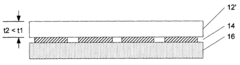
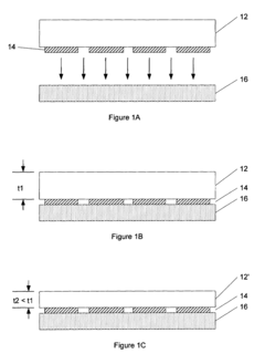
- A process involving sorting and batch processing of standard wafer blanks by thickness, followed by grinding and polishing to achieve a precise edge profile and final thickness of 400 microns with a total thickness variation of less than one micron and average roughness of less than 50 nm, using a double side lapping machine with diamond particle abrasives and specific polishing templates.
Three inch silicon carbide wafer with low warp, bow, and TTV
PatentActiveUS7422634B2
Innovation
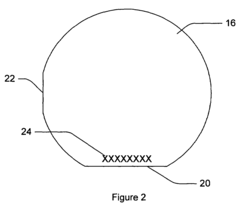
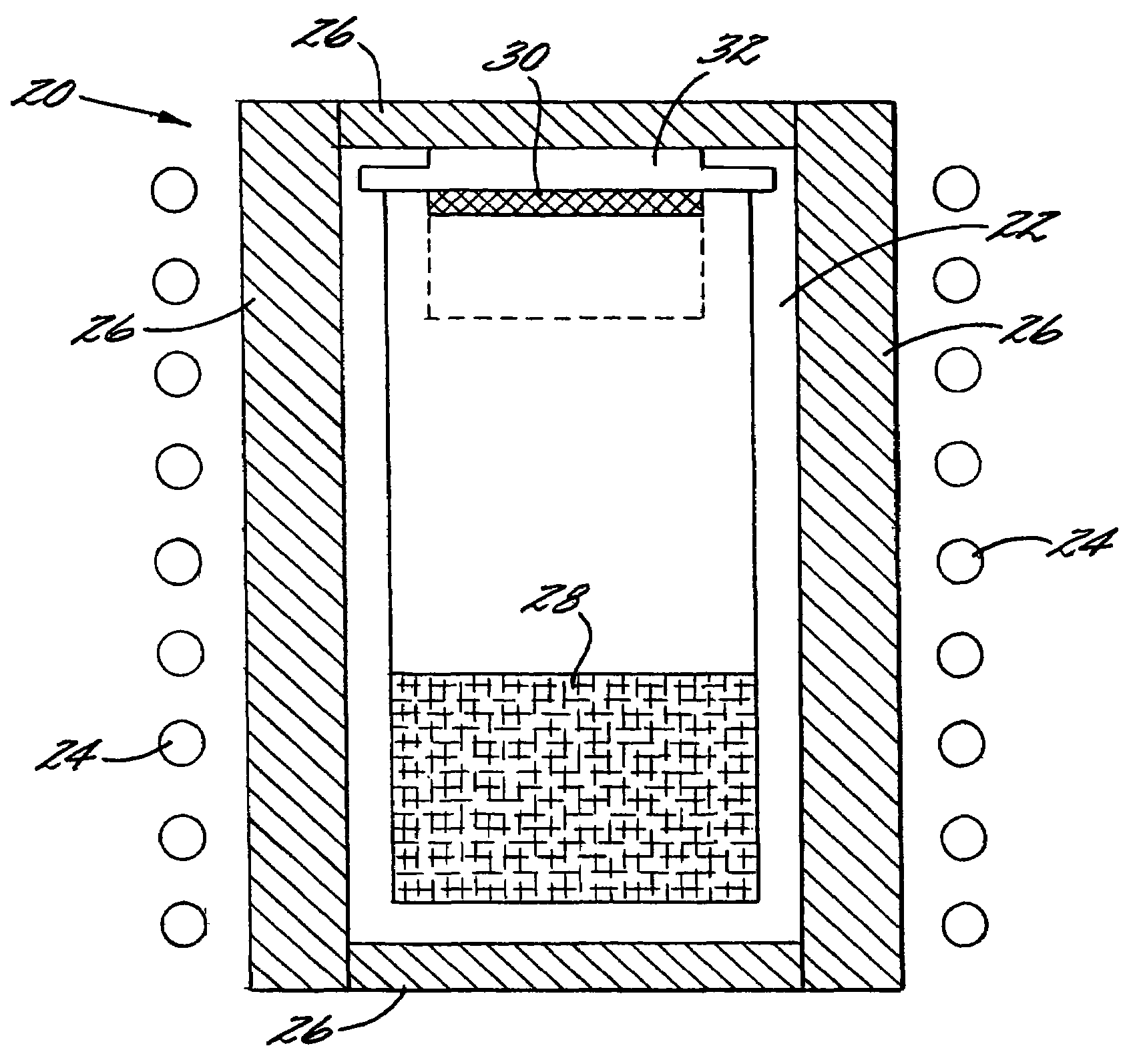
- The development of a method for producing high-quality silicon carbide wafers with diameters of at least 3 inches, featuring warp, bow, and TTV of less than 0.5 μm, 0.5 μm, and 1.0 μm respectively, using a seeded sublimation growth process with improved slicing and lapping techniques, including the use of a double-sided lapping machine and chemo-mechanical polishing to minimize surface and subsurface damage.

Material Properties Impact on Optimal Thickness
The intrinsic material properties of silicon carbide (SiC) play a decisive role in determining the optimal thickness parameters for wafer manufacturing. SiC exhibits exceptional thermal conductivity (approximately 370-490 W/m·K), which is significantly higher than silicon (148 W/m·K). This property enables more efficient heat dissipation in power devices, but simultaneously creates challenges during wafer thinning processes due to thermal gradient management requirements.
The mechanical strength of SiC, characterized by its Young's modulus of approximately 410-510 GPa (compared to silicon's 130-185 GPa), provides superior structural integrity even at reduced thicknesses. However, this same hardness property introduces significant challenges in mechanical processing operations, requiring specialized equipment and techniques for thinning and polishing processes.
Crystal structure variations between different SiC polytypes (primarily 4H-SiC and 6H-SiC) demonstrate distinct electrical and thermal behaviors that directly influence optimal thickness determinations. The 4H polytype, with its wider bandgap (3.26 eV versus 3.0 eV for 6H-SiC), exhibits superior electrical performance characteristics at reduced thicknesses, making it the preferred choice for power electronics applications where thinner wafers are increasingly demanded.
Defect density distribution throughout the SiC crystal volume represents another critical material property affecting thickness optimization. Studies indicate that defect concentration typically decreases with distance from the seed crystal, suggesting potential advantages in maintaining specific minimum thickness thresholds to avoid high-defect regions. Micropipe defects, in particular, show non-uniform distribution patterns that must be considered when establishing thickness parameters.
The thermal expansion coefficient of SiC (approximately 4.0-4.5 × 10^-6/K) creates significant challenges during temperature-dependent processing steps, especially when bonded to substrates with different expansion characteristics. This property necessitates careful thickness calculations to minimize wafer bow and warp during high-temperature manufacturing processes.
Electrical resistivity variations across the wafer thickness present another important consideration. Research demonstrates that resistivity profiles are non-uniform through the vertical dimension of SiC wafers, with implications for device performance when targeting specific thickness ranges. This non-uniformity must be carefully mapped and accounted for when establishing optimal thickness parameters for particular application requirements.
The mechanical strength of SiC, characterized by its Young's modulus of approximately 410-510 GPa (compared to silicon's 130-185 GPa), provides superior structural integrity even at reduced thicknesses. However, this same hardness property introduces significant challenges in mechanical processing operations, requiring specialized equipment and techniques for thinning and polishing processes.
Crystal structure variations between different SiC polytypes (primarily 4H-SiC and 6H-SiC) demonstrate distinct electrical and thermal behaviors that directly influence optimal thickness determinations. The 4H polytype, with its wider bandgap (3.26 eV versus 3.0 eV for 6H-SiC), exhibits superior electrical performance characteristics at reduced thicknesses, making it the preferred choice for power electronics applications where thinner wafers are increasingly demanded.
Defect density distribution throughout the SiC crystal volume represents another critical material property affecting thickness optimization. Studies indicate that defect concentration typically decreases with distance from the seed crystal, suggesting potential advantages in maintaining specific minimum thickness thresholds to avoid high-defect regions. Micropipe defects, in particular, show non-uniform distribution patterns that must be considered when establishing thickness parameters.
The thermal expansion coefficient of SiC (approximately 4.0-4.5 × 10^-6/K) creates significant challenges during temperature-dependent processing steps, especially when bonded to substrates with different expansion characteristics. This property necessitates careful thickness calculations to minimize wafer bow and warp during high-temperature manufacturing processes.
Electrical resistivity variations across the wafer thickness present another important consideration. Research demonstrates that resistivity profiles are non-uniform through the vertical dimension of SiC wafers, with implications for device performance when targeting specific thickness ranges. This non-uniformity must be carefully mapped and accounted for when establishing optimal thickness parameters for particular application requirements.
Manufacturing Cost vs Performance Trade-offs
The manufacturing cost of silicon carbide (SiC) wafers is significantly influenced by wafer thickness parameters, creating a complex trade-off relationship with performance characteristics. Thinner SiC wafers (typically below 350μm) require more sophisticated handling equipment and processing techniques, increasing manufacturing costs by approximately 15-25% compared to standard thickness wafers. However, these thinner substrates offer superior thermal dissipation properties, with thermal resistance decreasing by approximately 8-12% for every 50μm reduction in thickness, directly enhancing device performance in high-power applications.
Production yield represents another critical cost factor affected by wafer thickness. Current industry data indicates that ultra-thin wafers (<200μm) experience yield losses of 12-18% higher than standard thickness wafers due to increased susceptibility to warping, cracking, and handling damage during processing. These yield reductions directly impact per-unit costs, with some manufacturers reporting cost increases of up to 30% for finished devices on ultra-thin substrates.
The economic equation becomes more favorable when considering downstream benefits. Devices manufactured on optimized-thickness SiC wafers demonstrate 10-15% better power handling capabilities and 7-12% improved thermal performance, extending operational lifetimes by an estimated 20-30% in demanding applications. This performance enhancement can justify the higher initial manufacturing costs through improved total cost of ownership for end users, particularly in electric vehicles, renewable energy systems, and industrial power applications.
Material utilization efficiency presents another dimension of this trade-off. Advanced wafering technologies like multi-wire sawing can now produce more wafers per ingot when targeting reduced thickness specifications, potentially offsetting some manufacturing cost increases. Industry leaders have reported material utilization improvements of 8-14% when implementing optimized thin-wafer production processes, though these benefits are partially counterbalanced by higher equipment investment requirements.
The economic inflection point appears to occur around 350-375μm thickness for 6-inch wafers in current manufacturing environments, where production costs and performance benefits achieve optimal balance. However, this equilibrium continues to shift as manufacturing technologies evolve, with projections suggesting the cost-optimal thickness may decrease to 300-325μm by 2025 as handling and processing technologies mature, potentially unlocking new application domains where SiC adoption was previously limited by cost constraints.
Production yield represents another critical cost factor affected by wafer thickness. Current industry data indicates that ultra-thin wafers (<200μm) experience yield losses of 12-18% higher than standard thickness wafers due to increased susceptibility to warping, cracking, and handling damage during processing. These yield reductions directly impact per-unit costs, with some manufacturers reporting cost increases of up to 30% for finished devices on ultra-thin substrates.
The economic equation becomes more favorable when considering downstream benefits. Devices manufactured on optimized-thickness SiC wafers demonstrate 10-15% better power handling capabilities and 7-12% improved thermal performance, extending operational lifetimes by an estimated 20-30% in demanding applications. This performance enhancement can justify the higher initial manufacturing costs through improved total cost of ownership for end users, particularly in electric vehicles, renewable energy systems, and industrial power applications.
Material utilization efficiency presents another dimension of this trade-off. Advanced wafering technologies like multi-wire sawing can now produce more wafers per ingot when targeting reduced thickness specifications, potentially offsetting some manufacturing cost increases. Industry leaders have reported material utilization improvements of 8-14% when implementing optimized thin-wafer production processes, though these benefits are partially counterbalanced by higher equipment investment requirements.
The economic inflection point appears to occur around 350-375μm thickness for 6-inch wafers in current manufacturing environments, where production costs and performance benefits achieve optimal balance. However, this equilibrium continues to shift as manufacturing technologies evolve, with projections suggesting the cost-optimal thickness may decrease to 300-325μm by 2025 as handling and processing technologies mature, potentially unlocking new application domains where SiC adoption was previously limited by cost constraints.
Unlock deeper insights with PatSnap Eureka Quick Research — get a full tech report to explore trends and direct your research. Try now!
Generate Your Research Report Instantly with AI Agent
Supercharge your innovation with PatSnap Eureka AI Agent Platform!