Silicon Carbide Wafer Performance Benefits in Computational Devices
OCT 14, 20259 MIN READ
Generate Your Research Report Instantly with AI Agent
Patsnap Eureka helps you evaluate technical feasibility & market potential.
SiC Wafer Evolution and Performance Objectives
Silicon carbide (SiC) wafers represent a significant advancement in semiconductor materials, evolving from experimental curiosities to critical components in high-performance computational devices. The journey of SiC as a semiconductor material began in the early 1900s with its first synthesis, but it wasn't until the 1970s that researchers began seriously exploring its potential for electronic applications. The material's wide bandgap properties, approximately three times that of silicon, immediately suggested capabilities for high-temperature and high-power operations that conventional silicon could not achieve.
The evolution of SiC wafer technology has been marked by persistent challenges in crystal growth and defect reduction. Early SiC wafers suffered from high micropipe densities and limited diameters, constraining their commercial viability. The breakthrough came in the 1990s with the development of modified Lely process and seeded sublimation growth techniques, enabling the production of larger, higher-quality wafers with significantly reduced defect densities.
Recent advancements have focused on increasing wafer diameter from 2 inches to 6 inches and beyond, while simultaneously improving crystal quality. This scaling has been crucial for reducing manufacturing costs and enabling SiC's integration into mainstream semiconductor fabrication processes. The progression from research-grade materials to production-ready wafers has accelerated particularly in the last decade, with defect densities decreasing by orders of magnitude.
The primary performance objectives for SiC wafers in computational applications center on exploiting their inherent material advantages. With a thermal conductivity three times higher than silicon, SiC-based devices can dissipate heat more efficiently, allowing for higher operating temperatures without performance degradation. This translates directly to computational devices that can maintain stability under intense processing loads, particularly beneficial for data centers and high-performance computing environments.
Another critical objective is leveraging SiC's superior breakdown electric field strength—approximately ten times that of silicon—to create more compact, energy-efficient computational components. This property enables the design of smaller transistors that can operate at higher voltages, potentially increasing computational density while reducing power consumption—a key consideration as computational demands continue to grow exponentially.
The long-term technical trajectory for SiC wafers aims at achieving near-perfect crystal quality at commercially viable costs, with zero-defect wafers becoming the industry standard. Simultaneously, research is focused on optimizing doping profiles and interface characteristics to maximize carrier mobility and minimize parasitic resistances, directly enhancing computational speed and efficiency. As artificial intelligence and quantum computing applications emerge, SiC wafers are positioned to play a crucial role in next-generation computational architectures that demand unprecedented levels of performance and reliability.
Market Analysis for SiC-Based Computational Devices
The Silicon Carbide (SiC) semiconductor market is experiencing unprecedented growth, driven by the material's superior performance characteristics compared to traditional silicon. The global SiC market was valued at approximately $2.52 billion in 2022 and is projected to reach $7.18 billion by 2028, representing a compound annual growth rate of 19.2%. This growth trajectory is particularly significant for computational devices, where SiC offers substantial advantages in power efficiency and thermal management.
The demand for SiC-based computational devices is primarily fueled by three key market segments. First, the data center industry, which faces critical challenges in power consumption and cooling costs, is increasingly adopting SiC solutions to reduce operational expenses. SiC-based power components can decrease energy consumption by up to 30% compared to silicon alternatives, translating to millions in savings for large-scale operations.
Second, the high-performance computing (HPC) sector represents a rapidly expanding market for SiC technology. As computational demands intensify with applications like artificial intelligence and complex simulations, the thermal advantages of SiC become increasingly valuable. The HPC market is expected to grow at 20.5% annually through 2027, creating substantial opportunities for SiC integration.
Third, edge computing applications are emerging as a significant growth driver. The need for computational power in remote or space-constrained environments makes SiC's efficiency and reliability particularly attractive. Market research indicates that 75% of enterprise-generated data will be processed at the edge by 2025, up from 10% in 2018, representing a massive shift in computational architecture that favors SiC technology.
Regional analysis reveals that North America currently leads in SiC adoption for computational devices, holding approximately 42% of the market share. However, Asia-Pacific is expected to demonstrate the highest growth rate at 24.3% annually, driven by massive investments in semiconductor manufacturing capacity in countries like Japan, South Korea, and China.
Customer segmentation shows that while large technology corporations currently account for 68% of SiC computational device purchases, small and medium enterprises are increasingly adopting these solutions as prices gradually decrease. This democratization of access is expected to expand the market significantly in the coming years.
Pricing trends indicate that while SiC wafers currently command a premium of 3-4 times that of silicon wafers, this gap is narrowing by approximately 8-10% annually as manufacturing scales up and yields improve. Industry analysts predict price parity with high-performance silicon solutions could be achieved within the next decade, potentially triggering mass market adoption.
SiC Wafer Technology Status and Barriers
Silicon Carbide (SiC) wafer technology has advanced significantly over the past decade, yet continues to face substantial technical barriers that limit its widespread adoption in computational devices. Currently, commercial SiC wafers are predominantly available in 4-inch and 6-inch diameters, with 8-inch wafers still in early development stages. This size limitation represents a significant disadvantage compared to silicon wafers, which are routinely produced in 12-inch diameters, creating challenges for integration with existing semiconductor manufacturing infrastructure.
The crystal quality of SiC wafers remains a critical concern, with defect densities typically ranging from 10^2 to 10^4 cm^-2, significantly higher than those in silicon wafers. These defects include micropipes, dislocations, stacking faults, and basal plane dislocations that can severely impact device performance and reliability. Although micropipe densities have been reduced to near-zero levels in premium wafers, other defect types continue to plague the material.
Surface morphology issues present another substantial barrier, as SiC wafers often exhibit higher surface roughness than silicon counterparts. Current chemical-mechanical polishing techniques struggle to achieve the sub-nanometer surface roughness required for advanced computational applications, particularly for high-frequency devices where interface quality directly impacts performance.
Manufacturing yield represents perhaps the most significant economic barrier to widespread adoption. SiC crystal growth processes are inherently more complex than silicon, requiring temperatures exceeding 2000°C and precisely controlled growth conditions. The resulting low yields and high production costs translate to SiC wafer prices approximately 5-10 times higher than comparable silicon wafers, making economic justification difficult for all but the most performance-critical applications.
Geographical distribution of SiC wafer production capabilities remains highly concentrated, with leading manufacturers located primarily in the United States, Japan, and Europe. This concentration creates supply chain vulnerabilities and potential bottlenecks as demand increases. China has recently made significant investments to develop domestic SiC wafer production capabilities, but quality and volume remain behind industry leaders.
Substrate uniformity across larger wafer diameters presents ongoing challenges, with thickness variations and wafer bow/warp exceeding silicon standards. These non-uniformities complicate subsequent processing steps and can lead to yield losses during device fabrication. The thermal conductivity of SiC wafers, while theoretically excellent, often varies significantly across the wafer due to crystalline imperfections and dopant concentration variations.
Despite these barriers, SiC wafer technology continues to advance, driven by demand from power electronics, RF applications, and emerging computational device architectures that can leverage SiC's superior thermal and electrical properties.
Current SiC Integration Solutions for Computing
01 Crystal growth and defect reduction techniques
Various methods for growing high-quality silicon carbide crystals with reduced defects are essential for improving wafer performance. These techniques focus on controlling growth conditions, reducing micropipe density, and eliminating basal plane dislocations. Advanced growth processes like physical vapor transport (PVT) and modified Lely methods help achieve larger diameter wafers with fewer crystallographic defects, resulting in improved electrical and thermal performance of SiC devices.- Crystal growth and defect reduction techniques: Various methods for growing high-quality silicon carbide crystals with reduced defects are essential for improving wafer performance. These techniques focus on controlling crystal growth parameters, reducing micropipe defects, and enhancing structural uniformity. Advanced growth processes like physical vapor transport (PVT) and modified Lely methods help achieve higher quality crystals with fewer dislocations and defects, resulting in superior electrical and thermal performance of the final wafers.
- Surface processing and polishing methods: Surface processing techniques significantly impact silicon carbide wafer performance. Chemical-mechanical polishing (CMP), plasma etching, and other surface treatments are used to achieve atomically smooth surfaces with minimal subsurface damage. These processes reduce surface roughness, remove damaged layers, and prepare wafers for epitaxial growth or device fabrication. Optimized surface processing results in improved electrical characteristics, reduced leakage current, and enhanced device reliability.
- Doping and conductivity control: Controlling the electrical properties of silicon carbide wafers through precise doping is crucial for device performance. Various doping techniques, including ion implantation and in-situ doping during crystal growth, are used to achieve specific resistivity and carrier concentration profiles. The type and concentration of dopants (such as nitrogen for n-type and aluminum or boron for p-type) significantly affect the electrical characteristics, breakdown voltage, and switching performance of devices fabricated on these wafers.
- Thermal management and stability: Silicon carbide wafers exhibit exceptional thermal conductivity and stability, making them suitable for high-temperature and high-power applications. Various techniques are employed to optimize these thermal properties, including controlling polytype formation, managing thermal stress during processing, and enhancing heat dissipation capabilities. Improved thermal management leads to better device performance under extreme conditions, higher reliability, and extended operational lifetime of silicon carbide-based electronic components.
- Epitaxial growth techniques: Epitaxial layer growth on silicon carbide substrates is critical for device performance. Advanced epitaxial techniques like chemical vapor deposition (CVD) are used to grow high-quality, uniform epitaxial layers with controlled thickness and doping profiles. The quality of these epitaxial layers directly impacts device characteristics such as breakdown voltage, on-resistance, and switching speed. Innovations in epitaxial growth processes focus on reducing defects, improving uniformity, and enhancing the interface between the substrate and epitaxial layers.
02 Surface preparation and polishing methods
Surface preparation techniques significantly impact silicon carbide wafer performance. Chemical-mechanical polishing (CMP), plasma etching, and other surface treatments are used to achieve atomically smooth surfaces with minimal subsurface damage. These processes reduce surface roughness, remove scratches, and eliminate damaged layers caused by mechanical processing, resulting in improved device performance, reduced leakage current, and enhanced carrier mobility in epitaxial layers grown on the wafers.Expand Specific Solutions03 Doping and conductivity control
Controlling the electrical properties of silicon carbide wafers through precise doping is crucial for device performance. Various techniques for introducing dopants like nitrogen, aluminum, and boron are employed to achieve specific resistivity levels and carrier concentrations. Advanced methods include ion implantation, epitaxial doping, and in-situ doping during crystal growth. These processes enable the production of wafers with uniform electrical characteristics needed for high-performance power devices.Expand Specific Solutions04 Epitaxial growth optimization
Epitaxial layer growth on silicon carbide substrates is critical for device performance. Techniques to optimize epitaxial growth include controlling gas flow dynamics, temperature profiles, and precursor chemistry in CVD reactors. These methods focus on achieving uniform thickness, controlled doping profiles, and minimizing crystallographic defects in the epitaxial layers. High-quality epitaxial layers are essential for maximizing breakdown voltage, reducing on-resistance, and improving overall device reliability in power electronics applications.Expand Specific Solutions05 Wafer characterization and quality control
Advanced characterization techniques are employed to evaluate silicon carbide wafer quality and performance. Methods include X-ray topography, photoluminescence mapping, Raman spectroscopy, and electrical measurements to detect defects, assess crystal quality, and verify electrical properties. Non-destructive testing approaches help identify subsurface defects and monitor wafer uniformity. These characterization techniques enable manufacturers to establish quality control standards and correlate wafer properties with device performance, ensuring consistent production of high-performance silicon carbide wafers.Expand Specific Solutions
Leading SiC Wafer Manufacturers and Ecosystem
Silicon Carbide (SiC) wafer technology for computational devices is in a growth phase, with the market expanding rapidly due to superior performance benefits in power efficiency and thermal management. The global SiC market is projected to reach significant scale as adoption increases across automotive, industrial, and computing sectors. Leading players like Wolfspeed, STMicroelectronics, and RESONAC have established strong technological foundations, while companies such as Huawei, IBM, and Mitsubishi Electric are advancing applications. Chinese institutions including State Grid and various universities are accelerating research efforts, indicating the technology's strategic importance. The ecosystem shows varying maturity levels, with established manufacturers demonstrating commercial viability while newer entrants focus on specialized applications and manufacturing innovations to capture market share in this increasingly competitive landscape.
Wolfspeed, Inc.
Technical Solution: Wolfspeed is a global leader in silicon carbide (SiC) technology, offering a comprehensive portfolio of 150mm and 200mm SiC wafers specifically engineered for computational devices. Their proprietary manufacturing process creates ultra-high-purity SiC substrates with defect densities below 1 cm-2, enabling superior device performance. Wolfspeed's SiC wafers feature thermal conductivity exceeding 370 W/mK (3x higher than silicon), breakdown field strength of 2.8 MV/cm (10x higher than silicon), and bandgap of 3.26 eV (3x wider than silicon). These properties allow computational devices to operate at junction temperatures up to 200°C while maintaining reliability. Their latest generation of SiC wafers incorporates advanced epitaxial growth techniques that reduce basal plane dislocations by 80%, significantly enhancing long-term device stability and performance in high-power computing applications.
Strengths: Industry-leading SiC wafer quality with lowest defect density; Established manufacturing infrastructure for volume production; Comprehensive vertical integration from substrate to epitaxy. Weaknesses: Higher cost compared to traditional silicon wafers; Limited wafer diameter options compared to mature silicon technology; Supply constraints due to high market demand.
STMicroelectronics International NV
Technical Solution: STMicroelectronics has developed advanced silicon carbide (SiC) wafer technology specifically optimized for computational devices through their proprietary STPOWER SiC platform. Their technology utilizes 150mm SiC substrates with carefully engineered epitaxial layers featuring controlled doping profiles and reduced micropipe densities below 0.5 cm-2. ST's SiC wafers incorporate unique surface preparation techniques that improve interface quality between SiC and gate dielectrics, critical for computational device performance. Their manufacturing process includes specialized annealing steps that reduce point defects by approximately 70%, enhancing carrier mobility and reducing leakage currents. For computational applications, ST has developed specialized SiC wafer variants with optimized resistivity ranges (0.015-0.028 Ω·cm) that balance conduction losses with switching performance. Their SiC wafers enable power devices that operate at frequencies exceeding 100 kHz while maintaining efficiency above 98%, significantly outperforming silicon-based alternatives in computational power delivery systems.
Strengths: Established high-volume manufacturing capability; Strong integration with their own device fabrication ecosystem; Advanced quality control systems for consistent wafer performance. Weaknesses: More focused on power electronics applications than pure computational devices; Less vertical integration in SiC substrate production compared to some competitors; Relatively higher cost structure compared to silicon alternatives.
Critical Patents in SiC Wafer Manufacturing
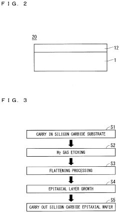
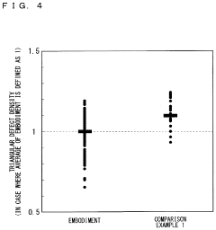
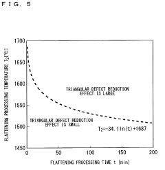
Method of manufacturing silicon carbide epitaxial wafer
PatentActiveUS20220028688A1
Innovation
- A method involving H2 gas etching at a specific temperature range, followed by flattening using SiH4 and C3H8 gases at a lower temperature, and epitaxial growth at an even lower temperature, ensuring that the etching temperature (T1) is greater than the flattening temperature (T2), which is greater than the growth temperature (T3), to efficiently remove latent flaws and inclusions and prevent triangular defects.
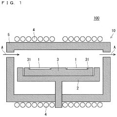
100 mm silicon carbide wafer with low micropipe density
PatentInactiveEP1807558A2
Innovation
- The development of high-quality silicon carbide wafers with diameters of at least 100 mm and micropipe densities of less than 25 cm^-2, achieved through optimized seeded sublimation growth processes, including the use of larger-diameter seed crystals, precise thermal gradients, and post-growth polishing and etching to reduce defects, allowing for the growth of bulk single crystals with improved polytype stability.
Thermal Management Advantages of SiC in Computing
Silicon Carbide (SiC) offers exceptional thermal management capabilities that significantly outperform traditional silicon in computational devices. With a thermal conductivity of approximately 370-490 W/m·K, SiC dissipates heat three times more efficiently than silicon, enabling more effective cooling in high-performance computing environments. This superior thermal performance allows computational devices to operate at higher power densities without reaching critical temperature thresholds.
The wide bandgap properties of SiC contribute to its thermal advantages, as the material can function reliably at temperatures exceeding 200°C, compared to silicon's practical limit of about 150°C. This temperature tolerance translates directly to reduced cooling requirements and simplified thermal management systems in data centers and high-performance computing facilities.
In practical applications, SiC-based power components in server farms demonstrate 30-45% reduction in cooling infrastructure requirements. The material's ability to operate efficiently at elevated temperatures allows for more compact heat sink designs and reduced fan speeds, contributing to overall energy savings and noise reduction in computing environments.
The thermal stability of SiC also enhances computational reliability. Temperature-induced performance degradation, a common challenge in silicon-based systems, occurs at a significantly reduced rate in SiC devices. Studies indicate that SiC-based computational components maintain consistent performance parameters across a wider temperature range, with junction temperature variations having 40% less impact on operational characteristics compared to silicon alternatives.
For edge computing and IoT applications, where passive cooling is often preferred, SiC offers compelling advantages. The material's thermal properties enable fanless designs for computational nodes deployed in harsh environments, extending operational lifespans by minimizing thermal cycling stress and reducing thermal-related failures by up to 60% compared to silicon-based alternatives.
From a system architecture perspective, SiC's thermal advantages enable more efficient power delivery networks in computational devices. The reduced thermal resistance between components allows for denser integration of processing units, memory, and power delivery systems, supporting the trend toward heterogeneous computing architectures where thermal constraints often limit performance scaling.
Advanced cooling techniques such as liquid cooling and immersion cooling demonstrate particularly strong synergy with SiC-based computational devices, further extending the thermal performance envelope and enabling computational densities previously unattainable with silicon technology.
Supply Chain Resilience for SiC Materials
The global supply chain for Silicon Carbide (SiC) materials faces unique challenges due to the specialized nature of production processes and limited supplier base. Currently, the SiC wafer supply chain is concentrated among a few key players, primarily in the United States, Europe, and Japan, creating potential vulnerabilities in global availability. The COVID-19 pandemic exposed these weaknesses, as disruptions in manufacturing and logistics led to significant delays in SiC wafer production and delivery, affecting computational device manufacturers worldwide.
Raw material sourcing represents a critical vulnerability point, as high-purity silicon carbide requires specific grades of silicon and carbon, often sourced from geographically concentrated regions. The complex manufacturing process, involving crystal growth at extremely high temperatures, further limits production capacity expansion and creates bottlenecks in the supply chain. These technical constraints have resulted in extended lead times, sometimes exceeding 6-9 months for specialized SiC wafers used in high-performance computational applications.
To enhance resilience, industry leaders are implementing multi-sourcing strategies, developing relationships with suppliers across different geographical regions to mitigate regional disruption risks. Companies like Wolfspeed, STMicroelectronics, and Infineon have announced significant investments in expanding their SiC production capacities across multiple locations, reducing dependency on single manufacturing sites. Additionally, vertical integration efforts are increasing, with some computational device manufacturers acquiring or investing in SiC wafer production capabilities to secure their supply.
Inventory management practices are evolving toward strategic stockpiling of critical SiC materials, balancing just-in-time manufacturing principles with supply security considerations. Advanced analytics and AI-driven supply chain monitoring tools are being deployed to predict potential disruptions and enable proactive mitigation measures. These systems analyze global supply chain data to identify emerging risks before they impact production schedules.
International collaboration initiatives are emerging to address supply chain vulnerabilities collectively. Industry consortia, government-backed programs, and public-private partnerships are working to establish more resilient supply networks for critical semiconductor materials, including SiC. The CHIPS Act in the United States and similar initiatives in Europe and Asia specifically target semiconductor supply chain resilience, with SiC materials identified as strategically important components.
Technological innovations in SiC wafer production, such as improved crystal growth techniques and more efficient manufacturing processes, are gradually increasing global production capacity while reducing dependency on specialized equipment. Research into alternative substrate materials and manufacturing methods continues to progress, potentially offering diversification options for computational device manufacturers in the longer term.
Unlock deeper insights with Patsnap Eureka Quick Research — get a full tech report to explore trends and direct your research. Try now!
Generate Your Research Report Instantly with AI Agent
Supercharge your innovation with Patsnap Eureka AI Agent Platform!