Patents Involving Silicon Carbide Wafer Manufacturing Innovations
OCT 14, 20259 MIN READ
Generate Your Research Report Instantly with AI Agent
Patsnap Eureka helps you evaluate technical feasibility & market potential.
SiC Wafer Manufacturing Evolution and Objectives
Silicon carbide (SiC) wafer manufacturing has evolved significantly since its inception in the early 20th century. Initially developed for abrasive applications, SiC has transformed into a critical semiconductor material for power electronics. The evolution began with the Acheson process in 1891, which provided industrial-scale SiC production but lacked the purity required for electronic applications. The technological breakthrough came in the 1950s with the Lely method, enabling the growth of higher-quality SiC crystals.
The 1970s and 1980s witnessed the development of seeded sublimation growth, also known as the modified Lely method, which became the foundation for modern SiC wafer production. This period marked the transition from research-scale to commercial-scale manufacturing capabilities, though wafer sizes remained limited to 1-2 inches with significant defect densities.
The 1990s represented a pivotal era with the introduction of physical vapor transport (PVT) techniques, enabling larger diameter wafers with improved quality. Companies like Cree (now Wolfspeed) pioneered commercial production during this period. The early 2000s saw further refinements in crystal growth processes, with wafer diameters expanding to 3-4 inches and defect densities decreasing by orders of magnitude.
Recent advancements from 2010 onward have focused on scaling to 6-inch and now 8-inch wafers while simultaneously addressing persistent challenges such as micropipe defects, basal plane dislocations, and polytype inclusions. Patent activity has intensified around innovations in seed crystal preparation, growth parameter optimization, and post-growth processing techniques to enhance yield and reduce manufacturing costs.
The primary objectives driving SiC wafer manufacturing innovation include increasing wafer diameter to achieve economies of scale comparable to silicon, reducing defect densities to improve device performance and reliability, enhancing crystal quality uniformity across the wafer, and developing more energy-efficient and cost-effective production methods. These objectives align with the growing demand for SiC-based power devices in electric vehicles, renewable energy systems, and industrial applications.
Current technological trajectories suggest continued focus on scaling to 8-inch and potentially 12-inch wafers, developing multi-wafer growth capabilities to increase throughput, and implementing advanced in-situ monitoring systems to provide real-time feedback during crystal growth. Additionally, significant research is directed toward alternative growth methods such as solution growth and continuous feed sublimation techniques that promise higher growth rates and improved crystal quality.
The evolution of SiC wafer manufacturing represents a critical enabling technology for the broader transition to more energy-efficient power electronics, with patent innovations serving as key indicators of technological progress and competitive positioning in this high-value semiconductor segment.
Market Analysis for SiC Wafer Applications
The Silicon Carbide (SiC) wafer market has experienced substantial growth in recent years, driven primarily by increasing demand in power electronics, electric vehicles, and renewable energy applications. The global SiC wafer market was valued at approximately $420 million in 2020 and is projected to reach $1.2 billion by 2026, representing a compound annual growth rate (CAGR) of 19.2% during the forecast period.
Power electronics represents the largest application segment for SiC wafers, accounting for nearly 60% of the total market share. This dominance stems from SiC's superior properties compared to traditional silicon, including higher breakdown electric field strength, thermal conductivity, and electron saturation velocity. These characteristics enable the development of more efficient and compact power devices that can operate at higher temperatures and voltages.
The automotive sector has emerged as the fastest-growing application area for SiC wafers, particularly in electric vehicle (EV) powertrains. Major automotive manufacturers including Tesla, BMW, and Toyota have begun incorporating SiC-based power modules in their EV models, resulting in improved range, faster charging capabilities, and reduced cooling requirements. Industry analysts predict that by 2025, over 40% of new EVs will utilize SiC power electronics.
Renewable energy applications, particularly solar inverters and wind power systems, constitute another significant market for SiC wafers. The implementation of SiC-based devices in these systems has demonstrated efficiency improvements of 2-3% compared to silicon-based alternatives, translating to substantial energy savings over system lifetimes. The industrial sector is also adopting SiC technology for motor drives, uninterruptible power supplies, and industrial automation equipment.
Geographically, Asia-Pacific dominates the SiC wafer market with approximately 45% market share, followed by North America and Europe. China has made significant investments in SiC manufacturing capabilities as part of its strategic focus on semiconductor self-sufficiency, while Japan maintains leadership in high-quality SiC substrate production.
Despite promising growth prospects, the SiC wafer market faces challenges including high manufacturing costs and defect densities compared to silicon wafers. The average selling price of a 6-inch SiC wafer remains 5-7 times higher than its silicon counterpart, though this price differential is gradually decreasing as manufacturing technologies improve and production scales increase.
Market forecasts indicate that demand for larger diameter SiC wafers (6-inch and 8-inch) will grow at a faster rate than smaller diameters, as device manufacturers seek to improve economies of scale. The transition from 4-inch to 6-inch wafers is already well underway, while 8-inch wafer technology is still in early commercialization phases but expected to gain significant market share by 2028.
Global SiC Wafer Technology Landscape and Barriers
The global Silicon Carbide (SiC) wafer technology landscape is characterized by significant regional disparities in development and manufacturing capabilities. North America, particularly the United States, maintains leadership in SiC wafer innovation with companies like Wolfspeed (formerly Cree), II-VI Incorporated, and GT Advanced Technologies holding substantial patent portfolios. These entities have established robust manufacturing infrastructures and continue to push technological boundaries in crystal growth techniques.
Europe represents another significant hub, with companies such as STMicroelectronics, Infineon Technologies, and SOITEC making substantial investments in SiC wafer technology. The European Commission has recognized SiC as a strategic material, supporting research initiatives through programs like Horizon Europe to strengthen the region's competitive position.
In Asia, Japan has historically maintained strong capabilities through corporations like Rohm Semiconductor and Showa Denko, while China has rapidly expanded its presence with aggressive investments in SiC manufacturing capacity. Chinese companies including SICC Materials and TankeBlue have emerged as important players, supported by national initiatives like "Made in China 2025" that specifically target semiconductor self-sufficiency.
Despite technological advancements, significant barriers impede broader SiC wafer adoption. The foremost challenge remains manufacturing cost, with SiC wafers typically costing 5-10 times more than silicon alternatives. This cost differential stems from complex manufacturing processes, lower yields, and smaller economies of scale compared to mature silicon technology.
Material quality issues present another substantial barrier. Defect densities in SiC wafers remain higher than in silicon counterparts, with micropipes, dislocations, and basal plane defects affecting device performance and reliability. Patent analysis reveals intensive research focused on defect reduction techniques, particularly for larger diameter wafers.
Scalability challenges persist as manufacturers struggle to produce larger diameter wafers (6-inch and beyond) with consistent quality. While 6-inch wafers have entered commercial production, 8-inch wafer technology remains primarily in the research domain, with patents revealing significant technical hurdles in crystal growth uniformity at larger diameters.
Equipment specialization represents another barrier, as conventional silicon wafer manufacturing equipment requires substantial modification for SiC processing. The extreme hardness of SiC necessitates specialized cutting, grinding, and polishing technologies, creating additional cost barriers for new market entrants.
Intellectual property concentration also limits market access, with key manufacturing processes protected by extensive patent portfolios held by established players. This concentration creates significant entry barriers for emerging companies without substantial R&D resources or licensing agreements.
Current SiC Wafer Production Methodologies
01 Silicon Carbide Wafer Manufacturing Methods
Various methods for manufacturing silicon carbide wafers have been developed to improve quality and yield. These methods include specific crystal growth techniques, cutting processes, and surface treatments that enhance the wafer's structural integrity and electrical properties. Advanced manufacturing processes help reduce defects and improve the overall performance of silicon carbide wafers for semiconductor applications.- Silicon Carbide Wafer Manufacturing Methods: Various methods for manufacturing silicon carbide wafers have been developed to improve quality and yield. These methods include specific growth techniques, cutting processes, and surface treatments that enhance the crystalline structure and reduce defects. Advanced manufacturing processes focus on producing larger diameter wafers with fewer imperfections, which are essential for high-performance semiconductor applications.
- Surface Treatment and Polishing Techniques: Surface treatment and polishing techniques are crucial for preparing silicon carbide wafers for device fabrication. These processes include chemical-mechanical polishing, etching, and planarization methods that reduce surface roughness and remove subsurface damage. Advanced polishing techniques help achieve atomically smooth surfaces with minimal defects, which is essential for subsequent epitaxial growth and device performance.
- Epitaxial Growth on Silicon Carbide Substrates: Epitaxial growth processes on silicon carbide substrates are essential for creating functional semiconductor layers. These techniques involve controlled deposition of thin crystalline films on SiC wafers under specific temperature and pressure conditions. Various methods such as chemical vapor deposition (CVD) and molecular beam epitaxy are employed to grow high-quality epitaxial layers with precise doping profiles for power electronics and optoelectronic applications.
- Defect Reduction and Quality Control: Techniques for reducing defects and improving quality control in silicon carbide wafers focus on minimizing crystallographic imperfections such as micropipes, dislocations, and stacking faults. These methods include thermal annealing, defect conversion processes, and specialized growth parameters that enhance wafer uniformity. Advanced characterization techniques are employed to detect and classify defects, ensuring higher yield and reliability for demanding applications.
- Silicon Carbide Wafer Applications in Power Electronics: Silicon carbide wafers are increasingly used in power electronics applications due to their superior properties compared to traditional silicon. These applications include high-voltage power devices, electric vehicle components, renewable energy systems, and industrial motor drives. SiC-based devices offer advantages such as higher operating temperatures, greater power density, faster switching speeds, and improved energy efficiency, making them ideal for next-generation power conversion systems.
02 Defect Reduction Techniques in SiC Wafers
Techniques for reducing defects in silicon carbide wafers focus on minimizing crystallographic imperfections such as micropipes, dislocations, and stacking faults. These methods include specialized annealing processes, epitaxial growth optimization, and defect conversion mechanisms. By reducing defects, the electrical performance and reliability of devices manufactured on these wafers can be significantly improved.Expand Specific Solutions03 Surface Processing and Polishing of SiC Wafers
Surface processing techniques for silicon carbide wafers include chemical-mechanical polishing, plasma etching, and thermal oxidation processes. These methods aim to achieve atomically smooth surfaces with minimal subsurface damage, which is crucial for subsequent device fabrication steps. Advanced polishing techniques help reduce surface roughness and remove damaged layers resulting from wafer slicing operations.Expand Specific Solutions04 Epitaxial Growth on SiC Substrates
Epitaxial layer growth on silicon carbide substrates involves controlled deposition of thin semiconductor films with specific electrical properties. Various techniques such as chemical vapor deposition (CVD) and molecular beam epitaxy are employed to grow high-quality epitaxial layers. The epitaxial process parameters, including temperature, pressure, and gas flow rates, are optimized to achieve desired doping profiles and minimize defects in the grown layers.Expand Specific Solutions05 SiC Wafer Applications in Power Electronics
Silicon carbide wafers are increasingly used in power electronic devices due to their superior properties compared to silicon, including higher breakdown voltage, thermal conductivity, and electron mobility. These wafers serve as substrates for manufacturing high-performance power devices such as MOSFETs, Schottky diodes, and IGBTs. The wide bandgap nature of silicon carbide enables devices to operate at higher temperatures, frequencies, and voltages, making them ideal for electric vehicles, renewable energy systems, and industrial applications.Expand Specific Solutions
Leading SiC Wafer Manufacturers and Competitive Dynamics
The silicon carbide (SiC) wafer manufacturing landscape is currently in a growth phase, with the market expanding rapidly due to increasing demand in electric vehicles, renewable energy, and 5G applications. The global competition is dominated by established players like Wolfspeed, which pioneered SiC technology, alongside RESONAC, SICC, and newer entrants from China. Technical maturity varies significantly across competitors, with Western companies generally possessing more advanced manufacturing capabilities and intellectual property portfolios. Chinese manufacturers are rapidly closing the gap through substantial investments and government support. The market is characterized by intensive patent activity around crystal growth techniques, defect reduction methods, and wafer processing innovations, reflecting the industry's focus on improving yield rates and reducing production costs to meet growing demand.
Wolfspeed, Inc.
Technical Solution: Wolfspeed has pioneered silicon carbide wafer manufacturing with their proprietary high-temperature chemical vapor deposition (CVD) process that enables the growth of high-quality 150mm and 200mm SiC wafers. Their patented technology focuses on reducing micropipe densities to below 1cm² and controlling basal plane dislocations through specialized thermal gradient techniques. Wolfspeed's innovations include the Zero-Micropipe (ZMP) wafer technology and advanced epitaxial growth processes that achieve uniform doping profiles across large-diameter wafers. Their manufacturing process incorporates automated defect detection systems that utilize AI-based image recognition to identify and categorize crystal defects during production, significantly improving yield rates. Recent patents cover methods for reducing stacking faults and controlling polytype inclusions during crystal growth, which has enabled them to achieve industry-leading material quality metrics.
Strengths: Industry-leading expertise in large-diameter SiC wafer production with superior crystal quality and lower defect densities. Established manufacturing infrastructure and extensive IP portfolio. Weaknesses: Higher production costs compared to silicon alternatives, and challenges in scaling to even larger diameters while maintaining quality consistency.
RESONAC CORP
Technical Solution: RESONAC (formerly Showa Denko) has developed advanced SiC wafer manufacturing technologies centered around their proprietary RAF (Repeated A-Face) growth method. This patented technique enables the production of ultra-high-quality 6-inch SiC wafers with significantly reduced crystal defects. Their innovation focuses on controlling the crystal growth interface through precise temperature and pressure management during the sublimation process. RESONAC's patents cover specialized seed crystal preparation methods that minimize propagation of basal plane dislocations and other defects into the grown crystal. Their manufacturing process incorporates automated X-ray topography systems for real-time defect monitoring and closed-loop control of growth parameters. Recent innovations include techniques for reducing residual stress in large-diameter wafers and specialized slicing methods that minimize kerf loss while improving surface quality, allowing for more efficient material utilization and higher yields in device manufacturing.
Strengths: Proprietary RAF technology enables production of high-quality, large-diameter wafers with industry-leading low defect densities. Strong vertical integration from material synthesis to wafer finishing. Weaknesses: Limited production capacity compared to some competitors, and challenges in cost reduction for mass market applications.
Key Patent Analysis in SiC Wafer Manufacturing
Process for producing wafer of silicon carbide single-crystal
PatentInactiveEP1752567B1
Innovation
- A process involving surface treatment of the silicon carbide single crystal wafers to remove machining damages, using a specific off-angle range of 0.4 to 1.2°, and optimizing the carbon to silicon feed ratio (C/Si) between 0.5 to 1.4 in the CVD process to achieve a flat epitaxial growth surface with reduced surface roughness and dislocation density.
Silicon carbide wafer and method of fabricating the same
PatentActiveUS11788204B2
Innovation
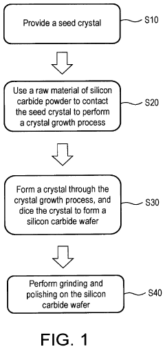
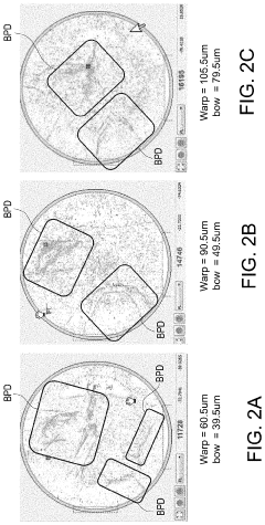
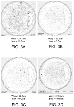
- A method for fabricating silicon carbide wafers that involves using a seed crystal with balanced basal plane dislocation defects and low impurity silicon carbide powder for crystal growth, ensuring minimal low angle grain boundaries within specific edge ranges, followed by grinding and polishing to achieve high flatness.
IP Strategy and Patent Portfolio Management
In the rapidly evolving landscape of silicon carbide (SiC) wafer manufacturing, strategic intellectual property management has become a critical competitive differentiator. Companies leading in this space have developed sophisticated patent portfolios that protect core innovations while enabling strategic market positioning. Analysis of patent filing trends reveals concentrated activity in key manufacturing process areas: crystal growth techniques, wafer slicing methodologies, surface polishing technologies, and defect reduction strategies.
The most successful organizations in SiC wafer manufacturing employ multi-layered IP strategies. Defensive patenting protects fundamental manufacturing processes, while offensive patents target emerging methodologies that competitors might develop. Companies like Cree/Wolfspeed, II-VI, and ROHM have established broad patent families covering multiple aspects of the manufacturing chain, creating significant barriers to entry for new market participants.
Geographic patent distribution shows strategic focus on key markets including the United States, Japan, Germany, and increasingly China. This reflects both manufacturing center locations and target market priorities. Forward-thinking companies are filing patents in emerging markets where SiC adoption is anticipated to grow rapidly in the next decade, particularly in regions developing electric vehicle and renewable energy infrastructure.
Patent portfolio management in this sector requires careful balance between protection breadth and depth. Leading manufacturers typically maintain 50-100 active patents specifically focused on wafer manufacturing processes, with renewal decisions based on technological relevance and market application potential. Strategic abandonment of patents for superseded technologies helps optimize portfolio management costs while maintaining protection for commercially valuable innovations.
Cross-licensing agreements have become increasingly common as the technology matures, allowing companies to access complementary technologies while monetizing their own innovations. These agreements often focus on specific manufacturing process steps rather than entire production chains, enabling companies to maintain competitive advantages in their areas of core expertise while accessing necessary peripheral technologies.
Future-focused IP strategies in this sector are increasingly incorporating trade secret protection alongside patent filings, particularly for process optimizations that deliver yield improvements or cost reductions. This hybrid approach recognizes that certain manufacturing innovations may deliver greater competitive advantage when kept confidential rather than disclosed through the patent system.
Environmental Impact of SiC Manufacturing Processes
Silicon carbide (SiC) wafer manufacturing processes, while offering significant technological advantages, present notable environmental challenges that warrant careful consideration. The production of SiC wafers involves energy-intensive processes that consume substantially more electricity than traditional silicon wafer manufacturing. The primary growth methods, including physical vapor transport (PVT) and chemical vapor deposition (CVD), require sustained high temperatures exceeding 2000°C, resulting in considerable carbon footprints when powered by non-renewable energy sources.
Water usage represents another significant environmental concern in SiC manufacturing. The processes demand ultra-pure water for cleaning and processing steps, with estimates suggesting that producing a single 6-inch SiC wafer may require between 5,000-8,000 gallons of water. This intensive consumption places pressure on local water resources, particularly in regions already experiencing water scarcity.
Chemical utilization in SiC manufacturing introduces additional environmental risks. The production processes employ various hazardous substances including silane gases, hydrogen chloride, and various metallic dopants. Without proper handling and treatment systems, these chemicals can contribute to air pollution, water contamination, and potential health risks for workers and surrounding communities.
Waste management challenges are particularly acute in SiC manufacturing. The processes generate solid waste including off-specification wafers, slurry waste from polishing operations, and spent abrasives. Additionally, the manufacturing creates hazardous byproducts such as silicon tetrachloride and various fluoride compounds that require specialized disposal protocols to prevent environmental contamination.
Recent patent innovations have begun addressing these environmental concerns. Several patents focus on closed-loop water recycling systems that can reduce freshwater consumption by up to 60%. Other innovations target energy efficiency through improved furnace designs and process optimization, potentially reducing energy requirements by 15-30% compared to conventional methods.
Emissions reduction technologies feature prominently in recent patent filings, with innovations in scrubber systems and abatement technologies specifically designed for SiC manufacturing exhaust streams. These systems can capture and neutralize harmful gases before release, significantly reducing air pollution impacts.
Material efficiency improvements represent another promising direction, with patents describing methods to reclaim and reuse silicon carbide from manufacturing waste. These approaches not only reduce waste volumes but also decrease the demand for raw materials, creating a more circular manufacturing ecosystem.
Unlock deeper insights with Patsnap Eureka Quick Research — get a full tech report to explore trends and direct your research. Try now!
Generate Your Research Report Instantly with AI Agent
Supercharge your innovation with Patsnap Eureka AI Agent Platform!