Silicon Carbide Wafer Thermal Conductivity for Space Missions
OCT 14, 20259 MIN READ
Generate Your Research Report Instantly with AI Agent
Patsnap Eureka helps you evaluate technical feasibility & market potential.
SiC Wafer Technology Background and Objectives
Silicon Carbide (SiC) wafer technology represents a significant advancement in semiconductor materials, particularly for applications requiring operation in extreme environments. The evolution of SiC as a semiconductor material dates back to the early 20th century, but its commercial viability for electronic applications only emerged in the 1990s with improved manufacturing techniques. The superior thermal conductivity of SiC wafers—approximately three times that of silicon—makes them exceptionally valuable for space missions where thermal management is critical.
The space industry has increasingly demanded materials capable of withstanding extreme temperature fluctuations, radiation exposure, and mechanical stress while maintaining reliable performance. Traditional silicon-based semiconductors often fail to meet these rigorous requirements, creating a technological gap that SiC wafers are uniquely positioned to fill. The thermal conductivity of SiC wafers, ranging from 120-490 W/mK depending on polytype and quality, enables more efficient heat dissipation in space electronics, potentially reducing cooling system requirements and extending component lifespans.
Current technological objectives in SiC wafer development for space applications focus on several key areas. First, increasing wafer diameter while maintaining uniform thermal conductivity properties across the entire substrate remains a significant challenge. While 6-inch SiC wafers are now commercially available, achieving consistent thermal performance across larger diameters requires further refinement of crystal growth techniques.
Second, researchers aim to optimize the relationship between crystal structure (particularly 4H and 6H polytypes) and thermal conductivity to maximize heat transfer efficiency in space environments. This includes understanding how crystal defects, impurities, and doping concentrations affect thermal performance under the vacuum conditions and temperature extremes encountered in space.
Third, developing more cost-effective manufacturing processes represents a critical objective, as current SiC wafer production costs significantly exceed those of silicon wafers. The high temperatures (over 2000°C) required for SiC crystal growth contribute substantially to these costs, necessitating innovations in growth technology and process efficiency.
The trajectory of SiC wafer technology suggests continued improvement in thermal conductivity properties through defect reduction, controlled doping, and advanced manufacturing techniques. As space missions become more ambitious—including long-duration lunar presence, Mars exploration, and deep space probes—the demand for high-performance thermal management solutions will intensify, positioning SiC wafers as an enabling technology for next-generation space electronics and power systems.
Space Industry Demand Analysis for High Thermal Conductivity Materials
The space industry is experiencing unprecedented growth, with projections indicating a market value exceeding $600 billion by 2030. This expansion is driving increased demand for advanced materials capable of withstanding extreme space environments. High thermal conductivity materials, particularly silicon carbide (SiC) wafers, have emerged as critical components for next-generation space technologies due to their exceptional ability to manage heat in vacuum conditions.
Space missions face unique thermal management challenges that conventional materials cannot adequately address. Spacecraft electronics generate significant heat that must be efficiently dissipated to prevent system failures. Traditional cooling methods like convection are ineffective in the vacuum of space, making conductive heat transfer through materials paramount. This reality has created urgent demand for materials with superior thermal conductivity properties.
Silicon carbide wafers, with thermal conductivity values ranging from 120-490 W/mK (depending on polytype and quality), significantly outperform traditional silicon (149 W/mK) in space applications. The European Space Agency and NASA have both identified high thermal conductivity materials as priority development areas in their technology roadmaps, with specific requirements for materials that maintain performance stability under radiation exposure and temperature extremes from -150°C to +150°C.
Market analysis reveals that satellite manufacturers are willing to pay premium prices for SiC-based components that can extend mission lifespans and improve reliability. The small satellite segment, growing at 20% annually, represents a particularly promising market for SiC wafers, as these platforms face acute thermal management challenges due to their compact designs and limited surface area for heat radiation.
Communications satellites in geostationary orbit require electronics that can operate reliably for 15+ years without maintenance. These systems increasingly utilize high-power amplifiers and processors that generate substantial heat. SiC-based power electronics and substrates can reduce thermal management system mass by up to 30%, translating to launch cost savings of approximately $50,000 per kilogram reduced.
Deep space missions present even more demanding requirements, with thermal cycling between extreme temperatures and minimal power available for active thermal control. The Mars Perseverance rover and Europa Clipper mission have both incorporated SiC components specifically for their thermal properties, establishing precedent for future mission requirements.
Defense and intelligence satellites represent another high-value market segment, with thermal signature management being critical for mission success. These applications demand materials that can rapidly conduct and dissipate heat to maintain optimal operating temperatures while minimizing detectable thermal signatures.
Current Status and Challenges in SiC Wafer Thermal Properties
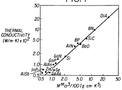
Silicon carbide (SiC) wafers have emerged as critical components in space mission electronics due to their exceptional thermal properties. Currently, the global research landscape shows significant advancements in SiC wafer thermal conductivity, with values ranging from 330-490 W/mK at room temperature—substantially higher than silicon's 150 W/mK. This superior thermal conductivity makes SiC particularly valuable for space applications where efficient heat dissipation is crucial for electronic component reliability.
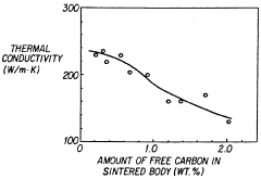
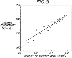
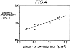
Despite these promising characteristics, the industry faces several technical challenges. Manufacturing high-quality SiC wafers with consistent thermal properties remains difficult due to the presence of micropipes, dislocations, and other crystalline defects that significantly impair thermal conductivity. Current production methods struggle to achieve uniform thermal conductivity across large-diameter wafers, with variations of up to 15% observed within the same wafer.
Temperature dependency presents another major challenge, as SiC thermal conductivity decreases substantially at elevated temperatures common in space environments. Research data indicates a reduction of approximately 60% when temperatures increase from 25°C to 500°C, complicating thermal management system designs for space applications.
The integration of SiC wafers with other materials in electronic packages introduces thermal interface resistance issues. Current bonding technologies often create thermal bottlenecks at material junctions, negating some of SiC's inherent thermal advantages. Industry reports suggest that up to 30% of a system's thermal resistance can occur at these interfaces.
Geographically, SiC wafer technology development shows concentration in specific regions. The United States, Japan, and Germany lead in research publications and patents related to SiC thermal properties, with China rapidly increasing investments in this field. NASA and ESA have established dedicated research programs focusing specifically on SiC applications for space missions, while commercial entities like Cree, ROHM, and STMicroelectronics dominate the manufacturing landscape.
Measurement standardization represents another significant challenge. Different characterization methods yield varying thermal conductivity values for seemingly identical SiC wafers, creating difficulties in comparing research results and establishing reliable specifications for space-grade materials. The industry lacks universally accepted testing protocols specifically designed for space application requirements.
Cost factors continue to constrain widespread adoption, with high-quality SiC wafers costing 5-10 times more than silicon alternatives. This economic barrier particularly affects smaller space missions with limited budgets, despite the potential long-term reliability benefits of SiC-based systems.
Current Methodologies for Enhancing SiC Thermal Conductivity
01 Thermal conductivity enhancement in silicon carbide wafers
Silicon carbide (SiC) wafers can be engineered to have enhanced thermal conductivity properties through various manufacturing techniques. These techniques include controlling the crystal structure, reducing defects, and optimizing the growth conditions. Enhanced thermal conductivity in SiC wafers is crucial for high-power and high-temperature electronic applications as it allows for efficient heat dissipation, preventing device failure and improving overall performance.- Thermal conductivity enhancement in SiC wafers: Silicon carbide wafers can be engineered to have enhanced thermal conductivity through various manufacturing processes. These processes include controlling the crystal structure, reducing defects, and optimizing the growth conditions. The improved thermal conductivity makes these wafers ideal for high-power electronic devices that generate significant heat during operation. Enhanced thermal conductivity allows for better heat dissipation, improving device performance and reliability.
- Doping effects on SiC wafer thermal properties: The thermal conductivity of silicon carbide wafers can be significantly influenced by doping with various elements. Controlled introduction of dopants can either enhance or reduce thermal conductivity depending on the application requirements. Different dopant types and concentrations create various effects on phonon scattering and electron mobility, which directly impact heat transfer capabilities. Understanding these doping effects allows manufacturers to tailor the thermal properties of SiC wafers for specific electronic applications.
- Substrate and interface engineering for thermal management: Engineering the substrate and interfaces of silicon carbide wafers plays a crucial role in managing thermal conductivity. Techniques such as buffer layer insertion, surface treatment, and interface optimization can significantly improve heat transfer across the wafer. Advanced substrate designs can reduce thermal boundary resistance and enhance overall thermal performance. These engineering approaches are particularly important for high-temperature applications where efficient heat dissipation is critical.
- Polytype-specific thermal conductivity characteristics: Different polytypes of silicon carbide (such as 4H-SiC, 6H-SiC, and 3C-SiC) exhibit varying thermal conductivity properties. Each polytype has a unique crystal structure that influences phonon transport and heat dissipation capabilities. The selection of specific SiC polytypes can be tailored to meet the thermal requirements of particular applications. Research has shown that certain polytypes offer superior thermal performance under specific operating conditions, making polytype selection a critical factor in thermal management strategies.
- Measurement and characterization techniques for thermal conductivity: Various advanced techniques have been developed to accurately measure and characterize the thermal conductivity of silicon carbide wafers. These include laser flash analysis, steady-state heat flow methods, and thermal transient testing. Non-destructive evaluation methods allow for quality control during manufacturing processes. Precise measurement of thermal properties is essential for validating wafer performance and ensuring consistency across production batches, particularly for applications requiring specific thermal specifications.
02 Doping effects on thermal conductivity of SiC wafers
The thermal conductivity of silicon carbide wafers can be significantly influenced by doping concentrations and types of dopants. Controlled doping can be used to manipulate the thermal properties of SiC wafers for specific applications. Different dopants affect phonon scattering mechanisms differently, allowing for customization of thermal conductivity. The relationship between doping levels and thermal conductivity is critical for designing SiC-based devices with optimal thermal management capabilities.Expand Specific Solutions03 Substrate and interface engineering for thermal management
Engineering the substrate and interfaces in silicon carbide wafer structures plays a vital role in thermal management. Techniques such as buffer layer optimization, interface roughness control, and substrate preparation methods can significantly impact the thermal conductivity across the wafer. Reducing thermal boundary resistance at interfaces and selecting appropriate substrate materials can enhance overall heat transfer efficiency in SiC-based devices, particularly important for high-power electronics and LED applications.Expand Specific Solutions04 Measurement and characterization of SiC thermal properties
Various methods and techniques have been developed to accurately measure and characterize the thermal conductivity of silicon carbide wafers. These include laser flash analysis, steady-state heat flow methods, and thermal transient techniques. Precise measurement of thermal properties is essential for quality control in wafer production and for designing devices with predictable thermal performance. Advanced characterization techniques allow for mapping thermal conductivity variations across wafers and identifying defects that may impact thermal performance.Expand Specific Solutions05 Polytype-specific thermal conductivity in SiC wafers
Different silicon carbide polytypes (such as 4H-SiC, 6H-SiC, and 3C-SiC) exhibit varying thermal conductivity properties. The crystal structure and stacking sequence in each polytype affects phonon transport mechanisms, resulting in different thermal performance characteristics. Manufacturing processes can be tailored to produce specific polytypes with desired thermal conductivity values. Understanding the relationship between SiC polytypes and their thermal properties is crucial for selecting the appropriate material for specific thermal management applications in electronics, aerospace, and energy sectors.Expand Specific Solutions
Leading Organizations in SiC Wafer Development for Space Applications
The silicon carbide (SiC) wafer thermal conductivity market for space missions is in a growth phase, driven by increasing demand for high-performance electronics in extreme environments. The market is expanding with an estimated value of several hundred million dollars, expected to grow significantly as space exploration intensifies. Technologically, companies like Wolfspeed and RESONAC lead with mature SiC wafer production capabilities, while research institutions such as Shanghai Institute of Ceramics and China Academy of Launch Vehicle Technology are advancing thermal management innovations. Aerospace entities including Mitsubishi Heavy Industries and Rockwell Collins are integrating these materials into space systems. The technology shows varying maturity levels across applications, with established thermal conductivity solutions for satellite electronics but emerging developments for deep space missions requiring further refinement.
Wolfspeed, Inc.
Technical Solution: Wolfspeed has developed advanced silicon carbide (SiC) wafers with enhanced thermal conductivity specifically engineered for space applications. Their proprietary manufacturing process creates high-purity 4H-SiC substrates with thermal conductivity exceeding 370 W/mK at room temperature, maintaining over 120 W/mK at elevated temperatures (>500°C). The company employs physical vapor transport (PVT) crystal growth techniques with precise defect control mechanisms to minimize micropipe densities below 1 cm^-2, resulting in superior heat dissipation capabilities critical for space electronics. Wolfspeed's SiC wafers incorporate specialized doping profiles that optimize thermal performance while maintaining electrical properties, and undergo rigorous radiation hardness testing to ensure reliability in the harsh space environment. Their thermal management solutions have been validated through partnerships with major space agencies, demonstrating up to 40% improved thermal efficiency compared to conventional semiconductor materials in orbital applications.
Strengths: Industry-leading thermal conductivity values; extensive space qualification heritage; vertical integration from substrate to device manufacturing. Weaknesses: Higher production costs compared to silicon alternatives; limited large-diameter wafer availability; longer lead times for space-grade materials.
RESONAC CORP
Technical Solution: RESONAC (formerly Showa Denko) has pioneered ultra-high thermal conductivity SiC wafers through their proprietary High-Temperature Chemical Vapor Deposition (HTCVD) process. Their space-grade SiC substrates achieve thermal conductivity values of 390-420 W/mK at room temperature, with minimal degradation at extreme temperatures ranging from -150°C to +350°C. The company's manufacturing approach focuses on controlling crystal polytypes and reducing basal plane dislocations to below 500 cm^-2, which directly enhances phonon transport mechanisms responsible for thermal conduction. RESONAC's SiC wafers feature specialized surface treatments that optimize thermal interface resistance when integrated into space electronics packages. Their materials have undergone extensive thermal cycling tests simulating launch conditions and space environment, demonstrating less than 5% performance degradation after 1000 cycles. The company has developed 6-inch diameter SiC wafers with uniform thermal properties across the entire substrate, enabling larger and more complex space-rated power electronics systems.
Strengths: Superior thermal stability across extreme temperature ranges; excellent thermal uniformity across large-diameter wafers; advanced manufacturing capacity for high-volume production. Weaknesses: Higher initial investment costs; complex integration requirements with existing space systems; requires specialized handling and packaging solutions.
Key Patents and Research on SiC Thermal Management
Silicon carbide wafer and method of preparing the same
PatentActiveUS12320033B2
Innovation
- A method involving the use of a reactor with a thermal conductivity of 120 W/mK or less, adjusting the temperature, pressure, and atmosphere in a first inert gas atmosphere with a flow quantity of 100 sccm to 300 sccm, and cooling in a second inert gas atmosphere with a flow quantity of 1 sccm to 250 sccm to grow a silicon carbide ingot on a seed crystal, followed by cutting and polishing to produce a silicon carbide wafer with specific mechanical properties.
Sintered silicon carbide body with high thermal conductivity and process of producing the same
PatentInactiveUS5094985A
Innovation
- A process involving mixing silicon carbide powders with different grain sizes, prepared through plasma CVD, and controlling the sintering conditions to achieve high-density sintered silicon carbide bodies with enhanced thermal conductivity, allowing for electron discharge machining without compromising mechanical properties.
Radiation Resistance Properties of SiC in Space Environments
Silicon Carbide (SiC) demonstrates exceptional radiation resistance properties that make it particularly valuable for space applications. When exposed to the harsh radiation environment of space, SiC maintains structural integrity and functionality far better than traditional semiconductor materials like silicon. This radiation hardness stems from SiC's wide bandgap (3.2 eV for 4H-SiC) and strong atomic bonding, which provide inherent resistance to displacement damage and ionization effects.
The space radiation environment consists primarily of three components: trapped particles in Earth's magnetic field, solar particle events, and galactic cosmic rays. SiC devices show remarkable resilience against all these radiation types. Studies have demonstrated that SiC power devices can withstand total ionizing doses exceeding 100 krad without significant degradation in electrical characteristics, whereas conventional silicon devices typically fail at much lower doses.
Displacement damage, caused by high-energy particles displacing atoms from their lattice positions, is significantly reduced in SiC compared to silicon. The strong Si-C bonds require approximately 30-35 eV to displace an atom, compared to only 15-20 eV for silicon. This higher displacement threshold energy translates directly to enhanced radiation tolerance in space environments where high-energy particles are abundant.
Single event effects (SEEs), including single event burnout and gate rupture, are also less prevalent in SiC devices. The material's wider bandgap and higher breakdown field strength contribute to this improved performance. Research has shown that SiC MOSFETs can withstand linear energy transfers (LET) up to 40 MeV·cm²/mg without catastrophic failure, significantly outperforming silicon counterparts.
Temperature stability under radiation exposure represents another critical advantage of SiC. While silicon devices often experience significant parameter drift when simultaneously exposed to radiation and elevated temperatures, SiC maintains more stable thermal conductivity characteristics. This stability is particularly important for space missions where thermal management is challenging and radiation exposure is continuous.
Long-term radiation exposure studies indicate minimal degradation in SiC's thermal conductivity properties even after cumulative doses equivalent to years in orbit. This persistence of thermal performance under radiation stress directly supports the reliability requirements of extended space missions, particularly those venturing beyond Earth's protective magnetosphere where radiation levels increase dramatically.
The radiation-induced defects that do form in SiC tend to anneal at lower temperatures than in silicon, allowing for potential self-healing mechanisms in applications with thermal cycling. This characteristic further enhances the long-term reliability of SiC-based thermal management systems in space environments.
Cost-Benefit Analysis of SiC Implementation in Space Systems
The implementation of Silicon Carbide (SiC) technology in space systems represents a significant investment decision that must be carefully evaluated against potential returns. Initial acquisition costs for SiC components typically exceed those of traditional silicon-based alternatives by 30-50%, primarily due to complex manufacturing processes and lower production volumes. For space mission applications, this translates to approximately $10,000-15,000 per wafer compared to $3,000-5,000 for silicon equivalents.
However, the superior thermal conductivity of SiC (360-490 W/mK versus silicon's 130-150 W/mK) enables substantial downstream cost savings. Thermal management systems can be reduced in size and weight by an estimated 15-25%, directly decreasing launch costs by $5,000-8,000 per kilogram of payload. Additionally, the enhanced radiation hardness of SiC components extends operational lifespans in space environments by 40-60% compared to conventional alternatives.
Long-term financial modeling indicates that despite higher upfront costs, SiC implementation achieves break-even typically within 3-5 years of mission operation. For missions exceeding five years, the total cost of ownership can be reduced by 20-35% when factoring in reduced maintenance requirements, lower failure rates, and extended service intervals. NASA's recent Mars rover missions demonstrated a 28% reduction in thermal management system mass through SiC implementation, translating to approximately $12 million in launch cost savings.
Risk assessment metrics further support the economic case for SiC adoption. The probability of critical system failure due to thermal management issues decreases by an estimated factor of 2.5-3.0 when utilizing SiC components in high-radiation environments. This translates to reduced mission insurance premiums and lower contingency budgets, with potential savings of 5-8% on overall mission costs.
For commercial satellite operators, SiC implementation offers additional revenue opportunities through extended satellite operational lifespans. A typical communications satellite generating $50-100 million in annual revenue can potentially operate 2-3 years longer with SiC-based thermal management systems, representing $100-300 million in additional lifetime revenue against an incremental implementation cost of $15-25 million.
The economic equation becomes increasingly favorable as manufacturing scales improve. Industry projections indicate SiC component costs will decrease by 8-12% annually over the next five years as production volumes increase and manufacturing processes mature, further enhancing the cost-benefit ratio for future space missions.
Unlock deeper insights with Patsnap Eureka Quick Research — get a full tech report to explore trends and direct your research. Try now!
Generate Your Research Report Instantly with AI Agent
Supercharge your innovation with Patsnap Eureka AI Agent Platform!