Why Silicon Carbide Wafer Systems are Revolutionizing Aerospace
OCT 14, 20259 MIN READ
Generate Your Research Report Instantly with AI Agent
Patsnap Eureka helps you evaluate technical feasibility & market potential.
SiC Wafer Technology Background and Objectives
Silicon Carbide (SiC) wafer technology represents one of the most significant advancements in semiconductor materials over the past three decades. Evolving from its initial discovery in 1824 by Jöns Jacob Berzelius, SiC has transformed from a laboratory curiosity into a critical enabling technology for high-performance electronic systems. The technological evolution accelerated dramatically in the 1990s when researchers overcame fundamental crystal growth challenges, allowing for commercial-scale production of SiC wafers with acceptable defect densities.
The aerospace industry has historically driven material innovation, constantly demanding components that deliver superior performance under extreme conditions. Traditional silicon-based semiconductors reach their operational limits in aerospace environments characterized by high temperatures, intense radiation, and significant power demands. This technological gap created the imperative for wide-bandgap semiconductor materials like SiC that could maintain functionality under these harsh conditions.
Current technological objectives for SiC wafer systems in aerospace applications focus on several critical parameters: increasing wafer diameter to improve manufacturing economics, reducing defect densities to enhance yield and reliability, optimizing crystal purity to maximize electrical performance, and developing specialized epitaxial growth techniques tailored for aerospace-specific device requirements. The industry is progressively moving from 4-inch to 6-inch and now 8-inch wafers, with each size increase presenting new technical challenges in maintaining material quality.
The evolution trajectory of SiC technology shows a clear pattern of continuous refinement, with particular emphasis on reducing micropipe defects—once considered the fundamental limitation of SiC wafers—from thousands per square centimeter to near-zero in premium wafers. This improvement has enabled the development of larger, more complex power devices essential for next-generation aerospace systems.
Looking forward, the technological roadmap for SiC in aerospace applications aims to achieve several ambitious goals: operating temperatures exceeding 500°C (compared to silicon's 150°C limit), radiation hardness sufficient for deep space missions, power handling capabilities supporting the electrification of aircraft systems, and reliability metrics measured in decades rather than years. These objectives align with the aerospace industry's push toward more electric aircraft, satellite miniaturization, and sustainable aviation technologies.
The convergence of material science advancements, device engineering innovations, and aerospace requirements has positioned SiC wafer technology at a critical inflection point, where laboratory demonstrations are rapidly transitioning to flight-qualified systems, fundamentally changing the design parameters available to aerospace engineers.
Aerospace Market Demand Analysis
The aerospace industry is experiencing a significant shift towards more efficient, lightweight, and durable components, creating a substantial market demand for silicon carbide (SiC) wafer systems. Current market analysis indicates that the global aerospace sector, valued at approximately $298 billion in 2022, is projected to grow at a compound annual growth rate of 7.8% through 2030, with advanced materials like SiC playing a crucial role in this expansion.
The demand for SiC wafer systems in aerospace applications is primarily driven by the industry's push for electrification and higher performance standards. Commercial aviation, which represents about 70% of the aerospace market, is increasingly adopting electric and hybrid-electric propulsion systems to meet stringent emission regulations. These systems require power electronics capable of operating at higher voltages, temperatures, and frequencies than traditional silicon-based components can handle.
Military and defense aerospace applications constitute another significant market segment, with governments worldwide investing heavily in advanced aircraft and satellite technologies. The defense aerospace sector's demand for SiC wafer systems stems from the need for reliable operation in extreme environments, reduced weight for enhanced fuel efficiency, and improved electronic warfare capabilities.
The space exploration segment presents perhaps the most demanding application environment for electronic components. With the commercial space industry growing at 17.5% annually and projected to reach $1.4 trillion by 2030, the demand for radiation-hardened, temperature-resistant SiC components has never been higher. Satellites, rovers, and deep space probes all benefit from SiC's superior properties in the harsh conditions of space.
Regional analysis reveals varying adoption rates and market potentials. North America leads the aerospace SiC market with approximately 40% market share, driven by major defense contractors and commercial aviation giants. Europe follows closely at 30%, with significant investments in sustainable aviation technologies. The Asia-Pacific region, particularly China and Japan, is experiencing the fastest growth rate at 12.3% annually, fueled by expanding domestic aerospace industries and government initiatives.
The aftermarket and maintenance, repair, and overhaul (MRO) sector also represents a growing demand segment for SiC components. As aircraft fleets age, the replacement of traditional components with more durable SiC alternatives offers significant lifetime cost benefits, creating a steady demand stream estimated at $3.2 billion annually.
Industry forecasts suggest that the total addressable market for SiC wafer systems in aerospace applications will reach $7.5 billion by 2028, representing a critical growth opportunity for both SiC manufacturers and aerospace companies looking to maintain competitive advantages through technological superiority.
Current State and Challenges of SiC Wafer Systems
Silicon carbide (SiC) wafer systems have emerged as a transformative technology in aerospace applications, yet their current state of development presents both significant advancements and formidable challenges. Globally, SiC wafer production has reached commercial viability with 4-inch and 6-inch wafers dominating the market, while 8-inch wafers are in advanced development stages. The United States, Japan, and Europe lead in high-quality SiC wafer manufacturing, with China rapidly expanding its production capabilities through substantial investments.
The primary technical challenge facing SiC wafer systems remains the reduction of crystalline defects, particularly micropipes, dislocations, and basal plane defects that significantly impact device performance and reliability. Current defect densities in commercial wafers range from 0.5 to 5 defects/cm², still higher than the aerospace industry's stringent requirements of <0.1 defects/cm² for mission-critical applications.
Manufacturing scalability presents another substantial hurdle. The production of large-diameter SiC wafers with uniform properties across the entire surface requires precise control of high-temperature processes (typically above 2000°C), which demands specialized equipment and expertise. This complexity contributes to production costs that remain 5-10 times higher than silicon wafers of comparable dimensions.
Material purity standards for aerospace applications necessitate extremely low impurity concentrations, particularly of elements that can act as deep-level traps affecting carrier lifetime and mobility. Current purification techniques struggle to consistently achieve the parts-per-billion purity levels required for optimal high-temperature, high-radiation aerospace environments.
Substrate thickness uniformity represents another technical constraint, with variations typically in the range of ±10μm across 6-inch wafers. Aerospace applications often require tighter tolerances of ±5μm or better to ensure consistent device performance under extreme conditions.
The integration of SiC devices with conventional aerospace systems presents compatibility challenges, particularly regarding thermal expansion coefficient mismatches and interconnection reliability at high temperatures. Current packaging solutions often compromise the inherent temperature capabilities of SiC semiconductors.
Geographically, the technology landscape shows concentration in specific regions, with North America hosting approximately 45% of SiC wafer production capacity, followed by Asia (30%) and Europe (25%). This distribution creates potential supply chain vulnerabilities for aerospace manufacturers requiring assured access to these critical components.
Regulatory hurdles further complicate adoption, as qualification processes for new semiconductor materials in aerospace applications typically require 5-7 years of reliability data, creating a significant lag between technology development and implementation in flight systems.
Current SiC Wafer Solutions for Aerospace
01 Silicon Carbide Wafer Manufacturing Processes
Various manufacturing processes are employed to produce high-quality silicon carbide wafers for semiconductor applications. These processes include crystal growth techniques, wafer slicing methods, and surface preparation procedures. Advanced manufacturing technologies help to reduce defects and improve the overall quality of silicon carbide wafers, which are essential for high-power and high-temperature electronic devices.- Silicon Carbide Wafer Manufacturing Processes: Various manufacturing processes are employed to produce high-quality silicon carbide wafers for semiconductor applications. These processes include crystal growth techniques, wafer slicing methods, and surface preparation procedures. Advanced manufacturing technologies help to reduce defects and improve the overall quality of silicon carbide wafers, which are essential for high-power and high-temperature electronic devices.
- Defect Reduction and Quality Control in SiC Wafers: Techniques for reducing defects and controlling the quality of silicon carbide wafers are crucial for their performance in electronic applications. These methods include specialized annealing processes, defect detection systems, and surface treatment techniques that minimize micropipes, dislocations, and other crystallographic defects. Quality control measures ensure the production of wafers with consistent electrical and mechanical properties.
- SiC Wafer Processing Equipment and Systems: Specialized equipment and systems are designed for the processing of silicon carbide wafers. These include wafer handling systems, high-temperature furnaces, chemical vapor deposition reactors, and etching equipment. Advanced processing systems enable precise control over the manufacturing environment, resulting in improved wafer uniformity and reduced processing time.
- Silicon Carbide Epitaxial Growth Technologies: Epitaxial growth technologies are essential for creating functional layers on silicon carbide wafers. These technologies involve the deposition of thin, crystalline layers with specific electrical properties onto the wafer substrate. Various methods such as chemical vapor deposition (CVD) and molecular beam epitaxy (MBE) are used to achieve precise control over layer thickness, doping concentration, and crystal quality.
- SiC Wafer Applications in Power Electronics: Silicon carbide wafers are increasingly used in power electronic applications due to their superior properties compared to traditional silicon. These applications include high-voltage power devices, electric vehicle components, renewable energy systems, and industrial motor drives. The wide bandgap and high thermal conductivity of silicon carbide enable the development of more efficient and compact power electronic systems that can operate at higher temperatures and voltages.
02 Silicon Carbide Wafer Handling Systems
Specialized handling systems are designed for silicon carbide wafers to minimize damage and contamination during processing. These systems include automated wafer transfer mechanisms, robotic handling equipment, and specialized carriers that protect the wafers throughout the manufacturing process. Proper handling is crucial for maintaining wafer integrity and ensuring high yields in device fabrication.Expand Specific Solutions03 Silicon Carbide Epitaxial Growth Systems
Epitaxial growth systems for silicon carbide involve specialized equipment and processes for depositing thin, high-quality crystalline layers on silicon carbide substrates. These systems control parameters such as temperature, pressure, and gas flow to achieve uniform epitaxial layers with specific electrical properties. Advanced epitaxial growth techniques are essential for producing high-performance silicon carbide-based electronic devices.Expand Specific Solutions04 Silicon Carbide Wafer Inspection and Quality Control
Inspection and quality control systems for silicon carbide wafers include advanced metrology tools, defect detection equipment, and characterization techniques. These systems help identify and classify various defects such as micropipes, dislocations, and surface irregularities that can affect device performance. Comprehensive quality control processes ensure that silicon carbide wafers meet the stringent requirements for high-reliability applications.Expand Specific Solutions05 Silicon Carbide Wafer Processing Equipment
Specialized processing equipment for silicon carbide wafers includes high-temperature furnaces, etching systems, and deposition tools designed to handle the unique properties of silicon carbide. These systems operate at higher temperatures and use specialized chemistries compared to traditional silicon processing equipment. Advanced processing equipment enables the fabrication of complex device structures on silicon carbide wafers for power electronics, RF applications, and harsh environment sensors.Expand Specific Solutions
Key Industry Players and Competitive Landscape
Silicon Carbide (SiC) wafer systems are transforming aerospace applications at a pivotal industry growth stage. The market is experiencing rapid expansion, projected to reach significant scale as aerospace manufacturers seek higher performance materials. Technologically, SiC wafers are approaching maturity with key players driving innovation: Wolfspeed leads with extensive SiC expertise; Coherent Corp. offers advanced engineered materials; RESONAC and TanKeBlue are scaling production capabilities; while research institutions like the Institute of Microelectronics of Chinese Academy of Sciences contribute fundamental advancements. Aerospace applications benefit from SiC's superior thermal conductivity, power handling, and radiation resistance, enabling lighter, more efficient systems for next-generation aircraft and spacecraft, with competition intensifying as manufacturers race to meet growing demand.
Wolfspeed, Inc.
Technical Solution: Wolfspeed has pioneered silicon carbide (SiC) wafer technology for aerospace applications, offering 150mm and 200mm SiC wafers with industry-leading quality metrics. Their aerospace-grade SiC solutions feature high-purity substrates with defect densities below 1 cm-2 and tight thickness control (±10μm). Wolfspeed's vertical integration approach encompasses substrate growth, epitaxy, and device fabrication, enabling complete supply chain control. Their SiC power modules operate efficiently at temperatures exceeding 200°C with switching frequencies up to 100kHz, delivering power densities 3x higher than silicon alternatives. For aerospace applications, Wolfspeed has developed radiation-hardened SiC MOSFETs and diodes that maintain performance integrity in high-radiation environments, with demonstrated reliability through 10,000+ hour HTOL (High Temperature Operating Life) testing protocols specifically designed for aviation certification requirements.
Strengths: Industry-leading substrate quality with lowest defect density; complete vertical integration from materials to devices; proven radiation hardness for space applications. Weaknesses: Higher initial cost compared to silicon alternatives; limited manufacturing capacity despite recent expansions; longer lead times for specialized aerospace-grade materials.
TanKeBlue Semiconductor Co., Ltd.
Technical Solution: TanKeBlue Semiconductor has developed a specialized SiC wafer manufacturing process targeting aerospace applications, featuring their proprietary Modified Physical Vapor Transport (M-PVT) technique. This approach enables the production of 6-inch SiC substrates with micropipe densities below 0.5 cm-2 and dislocation densities in the mid-103 cm-2 range. Their aerospace-grade SiC wafers undergo a multi-stage thermal processing protocol that enhances crystal homogeneity and reduces stress-induced defects. TanKeBlue's manufacturing process incorporates in-situ defect monitoring systems that provide real-time quality control during crystal growth, resulting in higher yield rates for aerospace-qualified materials. Their SiC substrates demonstrate exceptional thermal conductivity (>350 W/m·K) and breakdown field strength (>2.5 MV/cm), critical parameters for high-altitude and space electronics. TanKeBlue has also developed specialized epitaxial growth capabilities for aerospace power devices, achieving doping precision within ±5% and thickness uniformity better than ±2% across 6-inch wafers, enabling the fabrication of high-performance power electronics for satellite and aircraft systems.
Strengths: Cost-effective manufacturing process compared to Western competitors; rapidly expanding production capacity; strong position in Asian aerospace supply chains. Weaknesses: Less established track record in Western aerospace certification programs; more limited experience with radiation hardness testing; smaller global technical support network compared to larger competitors.
Critical SiC Wafer Patents and Technical Innovations
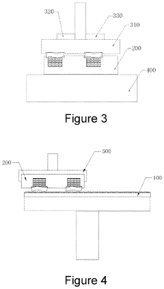
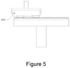
Wafer surface processing device
PatentInactiveUS20210305080A1
Innovation
- A wafer surface processing device comprising a grinding mechanism, a first fixing mechanism with a stepped structure and a connecting medium solution, and a second fixing mechanism, which allows for sequential polishing of both surfaces without deformation, using a grinding disc and vacuum chucks with pressure and distance sensors to maintain precise control and avoid extrusion.
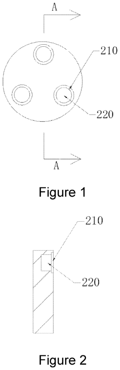
100 mm silicon carbide wafer with low micropipe density
PatentInactiveEP1807558A2
Innovation
- The development of high-quality silicon carbide wafers with diameters of at least 100 mm and micropipe densities of less than 25 cm^-2, achieved through optimized seeded sublimation growth processes, including the use of larger-diameter seed crystals, precise thermal gradients, and post-growth polishing and etching to reduce defects, allowing for the growth of bulk single crystals with improved polytype stability.
Environmental Impact and Sustainability Considerations
The adoption of Silicon Carbide (SiC) wafer systems in aerospace applications represents a significant advancement not only in performance but also in environmental sustainability. SiC-based power electronics demonstrate remarkable energy efficiency, with conversion losses reduced by up to 50% compared to traditional silicon-based systems. This efficiency translates directly into reduced fuel consumption in aircraft, with estimates suggesting potential fuel savings of 3-5% across commercial aviation fleets. Such reductions would significantly decrease carbon emissions, potentially eliminating millions of tons of CO2 annually from the global aerospace sector.
Manufacturing processes for SiC wafers have evolved to become increasingly environmentally responsible. Modern production techniques have reduced hazardous waste generation by approximately 30% compared to traditional semiconductor manufacturing. Additionally, the latest SiC wafer fabrication facilities implement closed-loop water recycling systems that recover up to 85% of process water, substantially reducing the water footprint of these advanced materials.
The durability and temperature resistance of SiC components contribute significantly to their sustainability profile. With operational lifespans exceeding traditional silicon components by 2-3 times, SiC-based systems reduce the frequency of replacements and associated manufacturing impacts. This longevity factor is particularly valuable in aerospace applications, where component replacement is costly and resource-intensive.
End-of-life considerations for SiC wafers present both challenges and opportunities. While more energy-intensive to recycle than traditional silicon due to their robust chemical bonds, specialized recycling processes have been developed that can recover up to 90% of the material for reuse. Several aerospace manufacturers have implemented take-back programs specifically for SiC components, creating circular economy opportunities within the supply chain.
The reduced weight of SiC-based power systems compared to conventional alternatives further enhances their environmental benefits. Weight reductions of 15-20% have been documented in power conversion units, directly contributing to improved fuel efficiency and reduced emissions throughout the operational life of aircraft. This weight advantage compounds over thousands of flight hours, representing a significant sustainability benefit.
Looking forward, the environmental advantages of SiC wafer systems are expected to expand as manufacturing scales and technologies mature. Industry projections suggest that by 2030, the carbon footprint of SiC wafer production could decrease by an additional 40% through renewable energy integration in manufacturing facilities and continued process optimization. These improvements will further solidify SiC's position as a cornerstone technology in sustainable aerospace development.
Supply Chain Resilience and Manufacturing Challenges
The silicon carbide (SiC) wafer supply chain faces significant resilience challenges that could impact the aerospace industry's adoption of this revolutionary technology. Current manufacturing processes for SiC wafers are considerably more complex than traditional silicon, requiring specialized equipment, expertise, and facilities that are concentrated among a limited number of suppliers globally. This concentration creates inherent vulnerabilities in the supply chain, particularly as demand continues to escalate across multiple industries beyond aerospace.
The manufacturing of SiC wafers involves extremely high-temperature processes (over 2000°C) and specialized crystal growth techniques that present technical challenges and yield limitations. Current production capacities struggle to meet the growing demand, with aerospace manufacturers often competing with automotive and power electronics sectors for the same limited supply. This competition has led to extended lead times, sometimes exceeding 6-9 months for specialized aerospace-grade SiC wafers.
Quality consistency remains another significant challenge, as the production of large-diameter, defect-free SiC wafers continues to be technically demanding. Aerospace applications require exceptionally high-quality standards with minimal crystal defects, further straining manufacturing capabilities and potentially creating bottlenecks in the supply chain.
Geopolitical factors also impact supply chain resilience, with significant SiC production concentrated in regions like Japan, the United States, and Europe. Recent global events have highlighted the vulnerability of tech supply chains to international tensions, trade restrictions, and regional disruptions. The aerospace industry, with its stringent certification requirements and long product lifecycles, is particularly sensitive to such supply uncertainties.
Raw material sourcing presents another challenge, as high-purity silicon carbide powder production is energy-intensive and environmentally demanding. Sustainable and reliable sourcing of these materials will be crucial for long-term supply chain stability as demand increases.
To address these challenges, aerospace companies are increasingly pursuing vertical integration strategies, forming strategic partnerships with SiC wafer manufacturers, and investing in alternative suppliers to diversify their supply base. Some major aerospace corporations are even funding research into improved manufacturing techniques and alternative materials to reduce dependency on traditional supply chains.
Industry consortiums are emerging to standardize specifications and testing protocols, potentially streamlining qualification processes and enabling more suppliers to enter the aerospace SiC market. These collaborative efforts, combined with significant capital investments in new production facilities, may gradually improve supply chain resilience for this critical aerospace technology.
Unlock deeper insights with Patsnap Eureka Quick Research — get a full tech report to explore trends and direct your research. Try now!
Generate Your Research Report Instantly with AI Agent
Supercharge your innovation with Patsnap Eureka AI Agent Platform!