Analysis of Silicon Carbide Wafer Durability in Harsh Conditions
OCT 14, 20259 MIN READ
Generate Your Research Report Instantly with AI Agent
Patsnap Eureka helps you evaluate technical feasibility & market potential.
SiC Wafer Evolution and Research Objectives
Silicon Carbide (SiC) wafers have emerged as a revolutionary material in the semiconductor industry, with their development tracing back to the early 1990s. Initially limited to small-diameter wafers with significant defect densities, SiC technology has undergone remarkable evolution over three decades. The progression from 2-inch to now commercially available 8-inch wafers represents a significant manufacturing achievement, overcoming numerous crystallization challenges inherent to this wide-bandgap material.
The harsh condition durability of SiC wafers stems from their fundamental material properties. With a bandgap of 3.2 eV (compared to silicon's 1.1 eV), SiC demonstrates exceptional thermal conductivity (3-4 times that of silicon), breakdown electric field strength (10 times higher), and inherent resistance to chemical corrosion. These properties position SiC as the material of choice for extreme environment applications where conventional silicon-based semiconductors would rapidly degrade or fail.
Current research objectives in SiC wafer technology focus on several critical dimensions. First, enhancing wafer durability under extreme temperature cycling conditions, particularly for aerospace and deep-well drilling applications where temperatures can fluctuate between -65°C and +600°C. Second, improving resistance to radiation damage for space and nuclear applications, where high-energy particle bombardment can compromise semiconductor integrity. Third, advancing chemical resistance properties for sensors and electronics deployed in highly corrosive industrial environments.
The technological trajectory indicates growing demand for larger-diameter wafers with reduced defect densities. Current state-of-the-art manufacturing achieves defect densities of approximately 0.1-0.5/cm², but applications in power electronics and quantum computing require further reduction to <0.01/cm². Additionally, wafer thickness uniformity remains a challenge, with variations currently at ±10μm needing improvement to ±2μm for next-generation applications.
Industry forecasts project the SiC wafer market to grow at a CAGR of 10.5% through 2030, driven primarily by electric vehicle adoption and renewable energy infrastructure. The research community is increasingly focused on developing standardized testing protocols for harsh condition performance, as current evaluation methods vary significantly across manufacturers and research institutions, complicating comparative analysis.
Our research objectives include quantifying SiC wafer performance degradation under combined stressors (thermal, chemical, mechanical, and radiation), identifying failure mechanisms at the crystalline level, and developing predictive models for wafer lifetime in specific harsh environments. These insights will inform both manufacturing process improvements and application-specific selection criteria for maximizing SiC wafer durability in mission-critical deployments.
Market Demand for Harsh-Condition Semiconductors
The global market for harsh-condition semiconductors has witnessed substantial growth in recent years, driven primarily by increasing demands in automotive, aerospace, energy, and industrial sectors. Silicon Carbide (SiC) wafers, with their superior thermal conductivity, high breakdown electric field strength, and wide bandgap properties, have emerged as critical components for applications operating in extreme environments.
Current market analysis indicates that the SiC semiconductor market is experiencing a compound annual growth rate (CAGR) exceeding 25%, with projections suggesting market valuation to reach beyond $3 billion by 2025. This growth trajectory is significantly steeper than that of conventional silicon-based semiconductors, reflecting the expanding application scope of SiC technology in harsh-condition environments.
The automotive sector represents the largest market segment for SiC wafers, particularly with the accelerating adoption of electric vehicles (EVs). SiC-based power electronics in EVs demonstrate superior efficiency in high-temperature engine compartments and power conversion systems, resulting in extended vehicle range and reduced charging times. Industry forecasts suggest that by 2026, over 60% of new EV models will incorporate SiC-based power electronics.
Industrial applications constitute another rapidly expanding market segment. Manufacturing facilities with extreme temperature variations, chemical exposure, and mechanical stress require semiconductor components with exceptional durability. The oil and gas industry, specifically, has increased investment in SiC-based sensing and control systems for downhole operations where temperatures can exceed 200°C and pressures reach 20,000 psi.
Aerospace and defense applications represent premium market segments where performance requirements justify higher component costs. SiC wafers enable reliable operation in radiation-exposed environments, extreme temperature fluctuations, and high-vibration conditions typical in aerospace applications. Military and space sectors are increasingly specifying SiC components for mission-critical systems.
Market research indicates significant regional variations in demand patterns. North America and Europe currently lead in adoption rates, primarily driven by automotive and aerospace applications. However, the Asia-Pacific region, particularly China, Japan, and South Korea, is demonstrating the fastest growth rate, supported by government initiatives to develop domestic semiconductor capabilities and rapid industrial automation.
Customer requirements are evolving toward thinner wafers with larger diameters (6-inch and 8-inch) to improve manufacturing economics while maintaining or enhancing durability specifications. This trend is creating market pressure for advanced manufacturing techniques that can produce larger-diameter SiC wafers without compromising their exceptional harsh-condition performance characteristics.
SiC Wafer Durability Challenges
Silicon carbide (SiC) wafers face significant durability challenges when deployed in harsh operating environments, which directly impact their performance and longevity. The primary challenge stems from the extreme temperature conditions these wafers must withstand. While SiC inherently possesses excellent thermal stability up to 1,700°C, prolonged exposure to thermal cycling between cryogenic and elevated temperatures induces mechanical stress that can lead to microcracking and eventual structural failure.
Chemical corrosion presents another formidable challenge, particularly in environments containing aggressive chemicals such as strong acids, bases, or oxidizing agents. Though SiC demonstrates superior chemical resistance compared to silicon, extended exposure to certain industrial chemicals can gradually degrade the wafer surface, compromising electrical properties and device performance. This is especially problematic in chemical processing applications and certain automotive environments.
Mechanical stress resistance represents a third critical challenge. SiC wafers must maintain structural integrity under high-pressure conditions and mechanical vibrations. The brittle nature of SiC makes it susceptible to fracturing under sudden impact or excessive mechanical loading, despite its high hardness. This vulnerability becomes particularly evident in applications involving frequent mechanical shocks or vibrations, such as aerospace and automotive systems.
Radiation hardness, while generally superior in SiC compared to silicon, still presents challenges in extreme radiation environments. High-energy particle bombardment can create defects in the crystal lattice, affecting carrier mobility and device characteristics. This becomes particularly relevant in space applications, nuclear facilities, and certain medical equipment where radiation exposure is unavoidable.
Manufacturing-related durability issues further complicate matters. Current SiC wafer production processes introduce various defects, including micropipes, dislocations, and stacking faults, which serve as weak points under harsh conditions. These inherent defects can propagate under stress, leading to premature failure. The challenge of producing defect-free SiC wafers at commercially viable costs remains significant.
Interface stability between SiC and other materials in device structures presents additional durability concerns. Thermal expansion coefficient mismatches between SiC and contact metals or insulating layers can lead to delamination or contact degradation during thermal cycling. This interfacial weakness often becomes the limiting factor in device reliability rather than the SiC material itself.
Long-term reliability under combined stressors represents perhaps the most complex challenge. Real-world applications rarely subject materials to isolated stress factors; instead, SiC wafers must simultaneously withstand combinations of thermal, chemical, mechanical, and electrical stresses. The synergistic effects of these combined stressors can accelerate degradation mechanisms in ways that are difficult to predict from single-factor testing protocols.
Current SiC Wafer Hardening Solutions
01 Surface treatment methods for enhancing durability
Various surface treatment methods can be applied to silicon carbide wafers to enhance their durability. These include chemical mechanical polishing, etching processes, and surface passivation techniques that reduce defects and improve mechanical strength. These treatments help to remove surface irregularities and create a more uniform surface structure, which contributes to increased wafer durability and resistance to mechanical stress during device fabrication.- Surface treatment methods for enhancing durability: Various surface treatment methods can be applied to silicon carbide wafers to enhance their durability. These include chemical mechanical polishing, plasma etching, and thermal oxidation processes that reduce surface defects and improve mechanical strength. These treatments create a more uniform surface structure that is less prone to cracking and degradation during device fabrication and operation, ultimately extending the wafer's usable lifetime and reliability in harsh environments.
- Crystal growth techniques for improved mechanical properties: Advanced crystal growth techniques can significantly improve the mechanical properties and durability of silicon carbide wafers. Methods such as physical vapor transport (PVT), modified Lely method, and continuous feed sublimation growth produce wafers with fewer defects, higher crystalline quality, and greater mechanical strength. These techniques focus on controlling the growth environment to minimize stacking faults, micropipes, and other crystallographic defects that would otherwise compromise wafer durability.
- Doping strategies to enhance wafer robustness: Strategic doping of silicon carbide wafers can enhance their mechanical robustness and durability. By incorporating specific dopants such as nitrogen, aluminum, or boron at controlled concentrations, the crystal structure can be strengthened while maintaining desired electrical properties. These doping strategies can reduce brittleness, increase fracture toughness, and improve resistance to thermal stress, making the wafers more durable during high-temperature processing and device operation.
- Protective coatings and buffer layers: Applying protective coatings and buffer layers to silicon carbide wafers can significantly enhance their durability. These include thin films of silicon dioxide, silicon nitride, or aluminum nitride that shield the wafer surface from mechanical damage, chemical attack, and thermal stress. Multi-layer buffer systems can also be employed to gradually transition between materials with different thermal expansion coefficients, reducing stress at interfaces and preventing crack formation during thermal cycling.
- Wafer handling and processing optimization: Optimizing wafer handling and processing techniques is crucial for maintaining silicon carbide wafer durability. This includes specialized equipment for wafer transport, customized fixtures for high-temperature processing, and modified cutting and grinding procedures that minimize edge chipping and surface damage. Advanced cleaning protocols that remove contaminants without etching or weakening the wafer surface also contribute to overall durability by preventing defect formation during subsequent processing steps.
02 Crystal growth techniques for improved mechanical properties
Advanced crystal growth techniques can significantly improve the mechanical properties and durability of silicon carbide wafers. Methods such as physical vapor transport (PVT), modified Lely method, and continuous feed sublimation growth produce high-quality SiC crystals with fewer defects and dislocations. These techniques result in wafers with enhanced structural integrity, higher fracture resistance, and improved overall durability for demanding applications.Expand Specific Solutions03 Doping and substrate modifications for durability enhancement
Introducing specific dopants and modifying the substrate composition can enhance the durability of silicon carbide wafers. Controlled doping with elements such as nitrogen, aluminum, or boron can improve mechanical properties while maintaining electrical characteristics. Additionally, engineered substrate structures with buffer layers or gradual compositional changes can reduce stress and prevent crack propagation, resulting in more durable wafers for high-temperature and high-power applications.Expand Specific Solutions04 Thermal processing techniques for durability optimization
Specialized thermal processing techniques can optimize the durability of silicon carbide wafers. These include high-temperature annealing, thermal oxidation, and controlled cooling processes that reduce internal stresses and heal crystal defects. Such thermal treatments can significantly improve the wafer's resistance to thermal cycling, mechanical shock, and chemical degradation, making them more suitable for harsh operating environments in power electronics and high-temperature applications.Expand Specific Solutions05 Protective coatings and encapsulation methods
Applying protective coatings and encapsulation methods can substantially enhance silicon carbide wafer durability. These include deposition of thin films such as silicon dioxide, silicon nitride, or advanced ceramic materials that protect the wafer surface from environmental factors, chemical attack, and mechanical damage. Multi-layer protective structures can be engineered to provide comprehensive protection while maintaining the wafer's electrical and thermal properties for long-term reliability in demanding applications.Expand Specific Solutions
Key SiC Wafer Manufacturers and Competitors
The silicon carbide wafer durability market is currently in a growth phase, with increasing demand driven by applications in harsh environments such as electric vehicles, power electronics, and aerospace. The global market is projected to expand significantly as SiC technology matures, offering superior thermal conductivity and chemical resistance compared to traditional silicon. Leading players include Wolfspeed, which dominates with advanced manufacturing capabilities, followed by RESONAC and GlobalWafers focusing on high-quality SiC substrate production. Other significant competitors include SICC, CoorsTek, and Tokai Carbon, each leveraging specialized expertise in material science. The technology is approaching maturity for power applications, though innovations in durability enhancement continue to emerge from research collaborations between industry leaders and institutions like University of Florida and Kyoto University.
Wolfspeed, Inc.
Technical Solution: Wolfspeed has pioneered advanced silicon carbide (SiC) wafer technology specifically engineered for harsh environment applications. Their proprietary high-purity SiC crystal growth process creates wafers with significantly reduced micropipe densities (<1 cm²) and improved crystalline uniformity[1]. Wolfspeed's 150mm and 200mm SiC wafers undergo specialized thermal oxidation treatments that enhance their durability under extreme temperature conditions (up to 600°C continuous operation). Their wafers feature proprietary edge treatment technology that reduces chipping and microcracking during high-stress processing and application. Additionally, Wolfspeed has developed specialized epitaxial growth techniques that create precisely controlled doping profiles, critical for maintaining electrical performance stability in harsh environments[3]. Their wafers demonstrate superior resistance to radiation damage, making them suitable for aerospace and nuclear applications, with testing showing functionality maintained after exposure to neutron fluences exceeding 10¹⁵ n/cm²[5].
Strengths: Industry-leading crystal quality with minimal defects; superior thermal stability allowing for higher operating temperatures than competitors; radiation hardness exceeding industry standards. Weaknesses: Higher production costs compared to silicon alternatives; limited production capacity affecting large-scale availability; longer manufacturing cycle times impacting market responsiveness.
RESONAC CORP
Technical Solution: RESONAC (formerly Showa Denko) has developed specialized silicon carbide wafer technology focused on harsh environment durability through their proprietary Advanced Chemical Vapor Deposition (CVD) process. Their SiC wafers feature ultra-high purity (>99.9999%) achieved through multiple purification steps and precise control of carbon-to-silicon ratios during crystal growth[2]. RESONAC's wafers undergo proprietary high-temperature annealing processes (>2000°C) that significantly reduce basal plane dislocations and point defects, resulting in enhanced mechanical strength under thermal cycling conditions. Their technology includes specialized surface passivation treatments that create protective oxide layers resistant to chemical corrosion in acidic and alkaline environments with pH ranges from 2-12[4]. RESONAC has also pioneered multi-layer epitaxial structures that distribute mechanical stress more effectively, improving wafer durability during rapid thermal cycling tests (demonstrated stability through >1000 cycles from -55°C to 350°C)[6]. Their wafers incorporate edge reinforcement technology that reduces susceptibility to edge chipping during handling and processing in industrial applications.
Strengths: Superior chemical resistance making their wafers ideal for corrosive environments; excellent thermal cycling stability; advanced defect management resulting in higher yield rates for device manufacturers. Weaknesses: Higher production costs compared to conventional silicon; more limited wafer diameter options than some competitors; relatively newer entrant to high-volume production compared to established leaders.
Critical Patents in SiC Wafer Durability
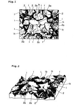
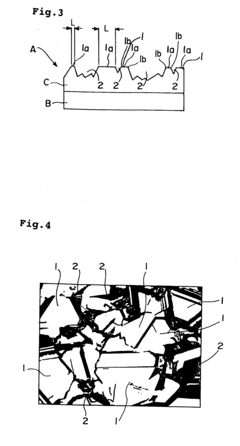
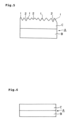
Chemical treatment to reduce machining-induced sub-surface damage in semiconductor processing components comprising silicon carbide
PatentInactiveUS20090142247A1
Innovation
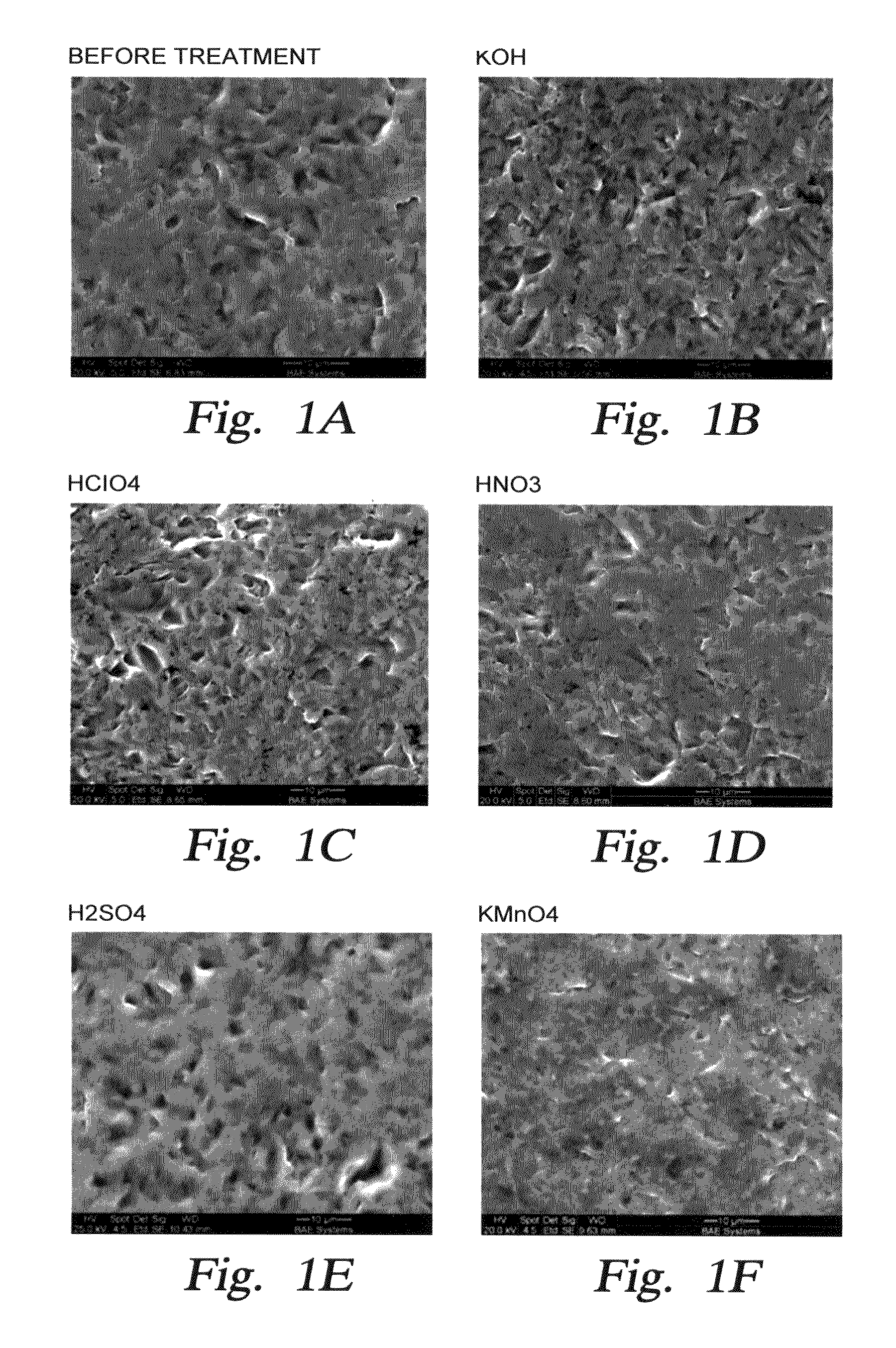
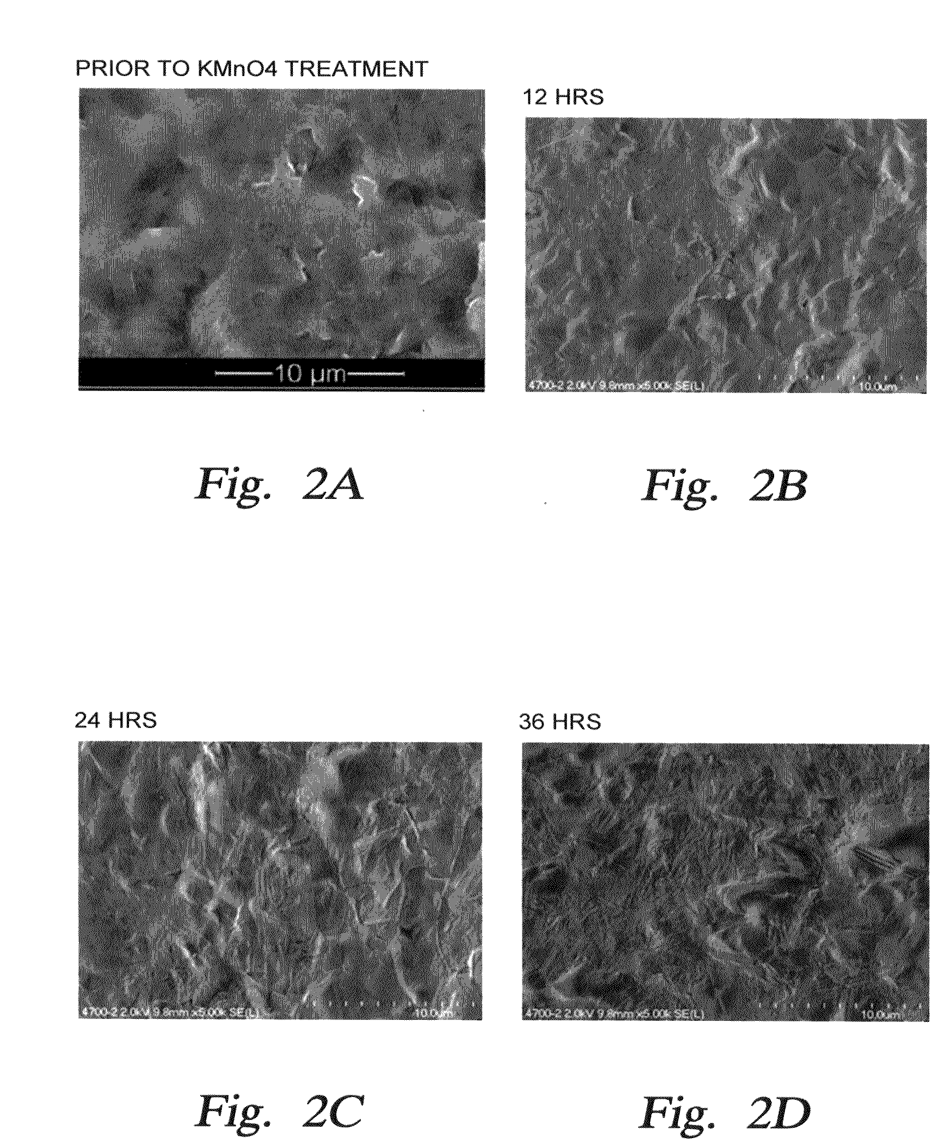
- A chemical solution treatment method involving multiple steps, including surface etching and exposure to liquid oxidizing agents like KMnO4, HNO3, or H2O2+H2SO4, followed by acid stripping to remove silicon oxide, effectively removes damaged crystalline structure from silicon carbide surfaces, reducing particulate generation and improving component lifetime.
Semiconductor wafer treatment member
PatentInactiveUS20040089236A1
Innovation
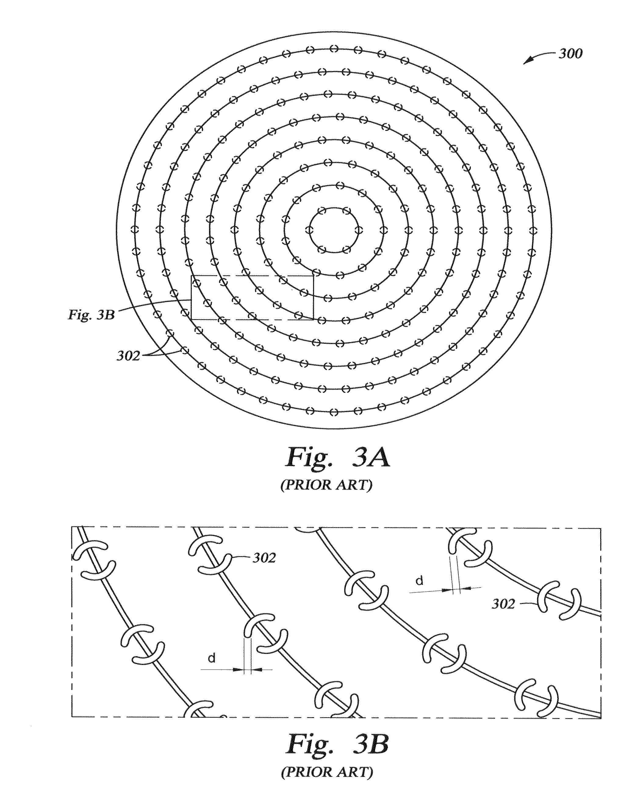
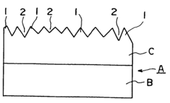
- A semiconductor wafer treatment member with a silicon carbide film featuring salients and depressions, where the surface roughness of the salients is between 0.05 μm to 1.3 μm, and the depressions cover 20 to 90% of the support area, reducing microcrack formation and enhancing cohesiveness while preventing contamination and thermal deformation.
Environmental Impact Assessment of SiC Manufacturing
The manufacturing of Silicon Carbide (SiC) wafers presents significant environmental considerations that must be thoroughly assessed. The production process involves high-temperature synthesis, typically exceeding 2000°C, which demands substantial energy consumption. This energy-intensive nature contributes considerably to carbon emissions, particularly when non-renewable energy sources power manufacturing facilities. A comprehensive life cycle assessment reveals that producing a single 6-inch SiC wafer can generate approximately 600 kg of CO2 equivalent emissions, substantially higher than traditional silicon wafer production.
Water usage represents another critical environmental concern. SiC manufacturing requires ultra-pure water for cleaning and processing, with estimates suggesting 5,000-7,000 liters of water consumption per wafer. The resulting wastewater contains various chemical compounds including hydrofluoric acid, heavy metals, and suspended solids that require specialized treatment before discharge to prevent ecosystem contamination.
Chemical utilization in SiC production introduces additional environmental challenges. The process employs hazardous substances such as silane gases, hydrogen chloride, and various solvents. These chemicals present potential risks through accidental releases, improper handling, or inadequate disposal practices. Particularly concerning is the use of perfluorinated compounds (PFCs) in certain etching processes, as these substances have extremely long environmental persistence.
Solid waste generation from SiC manufacturing includes silicon carbide particulates, spent abrasives, and damaged wafers. These materials often contain trace amounts of dopants and other processing chemicals that complicate recycling efforts. Current industry practices result in approximately 40-50% of raw materials becoming waste during the manufacturing process, highlighting significant inefficiency.
Land use impacts must also be considered, as manufacturing facilities require substantial space and often involve habitat disruption. The extraction of raw materials, particularly high-purity silica and carbon sources, contributes to mining-related environmental degradation in source regions.
Recent technological advancements have begun addressing these environmental concerns. Closed-loop water recycling systems can reduce freshwater consumption by up to 80%. Energy efficiency improvements through process optimization and equipment upgrades have demonstrated potential 15-25% reductions in energy requirements. Additionally, chemical substitution programs have successfully replaced some of the most environmentally problematic substances with more benign alternatives, though challenges remain in maintaining the required purity and performance characteristics essential for SiC wafer durability in harsh conditions.
Reliability Testing Methodologies for Harsh Environments
Reliability testing methodologies for silicon carbide (SiC) wafers in harsh environments require specialized approaches that go beyond standard semiconductor testing protocols. These methodologies must simulate extreme conditions while providing accurate, reproducible results that correlate with real-world performance. The testing framework typically encompasses thermal, mechanical, chemical, and electrical stress factors, often applied simultaneously to replicate actual operating environments.
Temperature cycling tests represent a cornerstone methodology, where SiC wafers undergo rapid transitions between temperature extremes (-65°C to 600°C) to evaluate thermal expansion coefficient mismatches and potential delamination issues. These tests typically follow standardized protocols such as JEDEC JESD22-A104 but with extended temperature ranges specific to SiC applications. The number of cycles often exceeds 1,000 to ensure statistical significance.
High-temperature operating life (HTOL) testing evaluates long-term reliability by subjecting wafers to elevated temperatures (typically 300-500°C for SiC) while under electrical bias. This methodology reveals degradation mechanisms that might not appear during normal qualification testing but emerge during extended field operation. Test durations typically range from 1,000 to 5,000 hours, with interim measurements to track progressive degradation.
Chemical resistance testing employs aggressive media exposure protocols, including acidic, alkaline, and oxidizing environments. SiC wafers are immersed in these solutions for predetermined periods, after which surface morphology, electrical characteristics, and mechanical properties are evaluated. This methodology is particularly relevant for applications in chemical processing industries and automotive sensors.
Mechanical stress testing incorporates vibration, shock, and pressure testing regimes. Vibration testing typically follows MIL-STD-883 Method 2007, but with customized profiles matching application-specific requirements. Shock testing evaluates wafer integrity under sudden acceleration events, while pressure cycling tests assess performance under varying atmospheric conditions.
Radiation hardness testing has become increasingly important for SiC applications in aerospace and nuclear environments. These methodologies expose wafers to controlled doses of gamma, neutron, or heavy ion radiation while monitoring electrical parameter drift. Post-irradiation electrical characterization reveals threshold voltage shifts, leakage current increases, and other radiation-induced effects.
Combined stress testing represents the most sophisticated reliability methodology, where multiple stressors are applied simultaneously. These tests often employ custom-designed chambers capable of creating harsh environments with precise control over temperature, humidity, chemical exposure, and electrical stress. While resource-intensive, these methodologies provide the most realistic assessment of SiC wafer durability in actual application environments.
Unlock deeper insights with Patsnap Eureka Quick Research — get a full tech report to explore trends and direct your research. Try now!
Generate Your Research Report Instantly with AI Agent
Supercharge your innovation with Patsnap Eureka AI Agent Platform!