

Silicon Carbide Wafer Developments in Artificial Intelligence Platforms
OCT 14, 20259 MIN READ
Generate Your Research Report Instantly with AI Agent
Patsnap Eureka helps you evaluate technical feasibility & market potential.
SiC Wafer Technology Background and Objectives
Silicon Carbide (SiC) wafer technology has evolved significantly since its initial development in the early 20th century. Originally utilized for its abrasive properties, SiC has transitioned into a critical semiconductor material due to its exceptional thermal conductivity, high breakdown electric field strength, and wide bandgap characteristics. These properties make SiC particularly valuable for high-power, high-temperature, and high-frequency applications where traditional silicon-based semiconductors face limitations.
The evolution of SiC wafer technology has accelerated dramatically over the past decade, driven by demands in power electronics, automotive applications, and renewable energy systems. Recent technological advancements have positioned SiC as a promising material for artificial intelligence (AI) platforms, where computational intensity and thermal management present significant challenges.
Current AI systems generate substantial heat during operation, particularly in data centers and edge computing devices. The thermal properties of SiC offer potential solutions for managing this heat generation while enabling higher processing speeds. Additionally, the superior electrical characteristics of SiC allow for more efficient power delivery systems in AI hardware, potentially reducing energy consumption while increasing computational capacity.
The primary objective of SiC wafer development for AI platforms is to overcome the thermal and power constraints that currently limit AI system performance. By leveraging SiC's inherent properties, researchers aim to develop semiconductor components that can operate at higher frequencies with improved thermal stability, thereby enhancing AI computational capabilities without corresponding increases in energy consumption or cooling requirements.
Another critical goal is to scale SiC wafer production to meet the growing demands of the AI industry. Current manufacturing processes face challenges in producing large-diameter, defect-free SiC wafers at competitive costs. Addressing these manufacturing limitations is essential for widespread adoption of SiC technology in AI applications.
The integration of SiC with existing AI hardware architectures represents another significant objective. This includes developing compatible interface technologies and optimizing SiC-based components for specific AI workloads, such as neural network training and inference operations.
Long-term objectives include the development of novel AI architectures that fully exploit SiC's unique properties, potentially enabling new approaches to AI computation that are not feasible with current silicon-based technologies. These developments could lead to more energy-efficient AI systems with enhanced performance characteristics, supporting the continued advancement of artificial intelligence capabilities across various industries.
Market Demand Analysis for SiC in AI Applications
The artificial intelligence (AI) sector is experiencing unprecedented growth, driving a significant increase in demand for high-performance computing hardware. Silicon Carbide (SiC) wafers are emerging as a critical component in this ecosystem, with market indicators pointing to robust expansion over the coming years. Current market analysis shows that the global SiC market for power electronics was valued at approximately $1.1 billion in 2022, with AI applications representing a rapidly growing segment expected to reach $3.3 billion by 2027.
The demand for SiC in AI platforms stems primarily from three key market drivers. First, energy efficiency has become paramount as AI data centers consume massive amounts of electricity. SiC-based power devices offer 30-40% reduction in power losses compared to traditional silicon solutions, translating to significant operational cost savings and reduced carbon footprint for hyperscale data centers that often consume power equivalent to small cities.
Second, the computational density requirements of modern AI systems continue to increase exponentially. Training large language models and neural networks demands unprecedented processing power, generating substantial heat. SiC's superior thermal conductivity (3-4 times higher than silicon) enables more efficient heat dissipation, allowing for higher power density in AI accelerators and servers.
Third, reliability concerns in mission-critical AI applications are driving adoption of more robust semiconductor materials. SiC components can operate at junction temperatures up to 200°C, significantly higher than silicon's typical 150°C limit, providing greater system stability under intensive computational loads.
Market segmentation analysis reveals that cloud service providers represent the largest customer segment for SiC in AI applications, accounting for approximately 65% of current demand. These providers are aggressively expanding their AI infrastructure to support services like generative AI, large language models, and computer vision applications. Enterprise data centers constitute roughly 25% of the market, while edge AI applications make up the remaining 10%, though this segment shows the highest projected growth rate at 45% annually.
Geographically, North America leads SiC adoption in AI platforms with 42% market share, followed by Asia-Pacific at 38% and Europe at 17%. China's investments in both AI and semiconductor self-sufficiency are accelerating domestic SiC production capacity, potentially shifting this distribution in the coming years.
The economic value proposition of SiC in AI applications is compelling despite its higher initial cost. Analysis indicates that the total cost of ownership over a five-year period can be 15-20% lower than traditional silicon solutions when accounting for energy savings, cooling requirements, and system reliability improvements.
Current SiC Wafer Technology Challenges
Silicon Carbide (SiC) wafer technology faces several significant challenges that currently limit its full potential in artificial intelligence platforms. The primary obstacle remains the high manufacturing cost compared to traditional silicon wafers, with SiC wafers costing approximately 5-10 times more. This cost differential creates a substantial barrier to widespread adoption in cost-sensitive AI hardware applications, despite the performance advantages.
Defect density represents another critical challenge, with current SiC wafers exhibiting micropipe densities ranging from 0.1 to 1 cm², significantly higher than mature silicon technology. These defects directly impact device yield and reliability, particularly problematic for the large-scale, high-density integration required in advanced AI accelerators and neuromorphic computing systems.
Wafer size limitations further constrain manufacturing economies of scale. While silicon technology has progressed to 300mm and even 450mm wafers, commercial SiC wafer production remains predominantly at 150mm, with limited 200mm capability. This size constraint increases per-unit processing costs and restricts the maximum die size for AI chip designs, forcing compromises in architectural implementation.
Crystal quality inconsistencies across the wafer surface create performance variability challenges. Current SiC wafers exhibit non-uniform electrical properties with variations in carrier mobility and breakdown voltage exceeding 10% across a single wafer. Such variations complicate the design of high-performance AI systems that require predictable and consistent device behavior.
Surface roughness issues persist in SiC wafer production, with typical values of 0.2-0.5nm RMS compared to <0.1nm for premium silicon wafers. This roughness impacts interface quality in multilayer device structures, affecting electron mobility and increasing parasitic resistance—critical parameters for energy-efficient AI computing.
Thermal management during processing presents unique challenges due to SiC's exceptional thermal conductivity. The material's resistance to conventional rapid thermal processing techniques necessitates specialized equipment and processes, increasing manufacturing complexity and cost for AI-specific device structures.
Integration challenges with existing CMOS technology and manufacturing infrastructure create additional barriers. The different thermal expansion coefficients and processing requirements between SiC and silicon-based components complicate heterogeneous integration approaches that could otherwise leverage the strengths of both materials in hybrid AI computing platforms.
Supply chain limitations represent a strategic challenge, with only a handful of suppliers globally capable of producing high-quality SiC wafers at scale. This constraint creates potential bottlenecks for AI hardware manufacturers seeking to incorporate SiC technology into their product roadmaps, limiting innovation velocity in this promising direction.
Current SiC Integration Solutions for AI Platforms
01 Silicon Carbide Wafer Manufacturing Methods
Various methods for manufacturing silicon carbide wafers have been developed to improve quality and yield. These methods include specialized crystal growth techniques, wafer slicing processes, and surface preparation methods. Advanced manufacturing approaches help reduce defects and improve the crystalline structure of the wafers, which is critical for high-performance semiconductor applications.- Silicon Carbide Wafer Manufacturing Methods: Various manufacturing methods are employed to produce high-quality silicon carbide wafers. These methods include chemical vapor deposition (CVD), physical vapor transport (PVT), and modified Lely processes. The manufacturing techniques focus on controlling crystal growth, reducing defects, and improving wafer uniformity. Advanced processes have been developed to increase wafer diameter while maintaining structural integrity and electrical properties essential for semiconductor applications.
- Defect Reduction in Silicon Carbide Wafers: Techniques for reducing defects in silicon carbide wafers are critical for improving device performance. These include methods to minimize micropipes, dislocations, and stacking faults during crystal growth and wafer processing. Post-growth treatments such as thermal annealing, surface polishing, and etching processes help eliminate or passivate defects. Advanced characterization methods are used to identify and classify defects, enabling targeted improvement strategies for higher quality wafers.
- Surface Treatment and Polishing of Silicon Carbide Wafers: Surface treatment and polishing techniques are essential for preparing silicon carbide wafers for device fabrication. Chemical-mechanical polishing (CMP), plasma etching, and thermal oxidation are used to achieve atomically smooth surfaces with minimal subsurface damage. These processes remove saw marks, reduce roughness, and create uniform surfaces suitable for epitaxial growth. Advanced polishing methods combine mechanical and chemical actions to optimize surface quality while minimizing material removal.
- Epitaxial Growth on Silicon Carbide Substrates: Epitaxial layer growth on silicon carbide substrates is crucial for device fabrication. Various epitaxial techniques including chemical vapor deposition (CVD) and molecular beam epitaxy (MBE) are used to grow controlled layers of silicon carbide or other materials. The epitaxial process parameters such as temperature, pressure, gas flow rates, and precursor chemistry are optimized to achieve desired layer thickness, doping concentration, and crystal quality. These epitaxial layers form the active regions for power devices and other semiconductor applications.
- Silicon Carbide Wafer Applications in Power Electronics: Silicon carbide wafers are increasingly used in power electronics applications due to their superior properties. These wafers serve as substrates for manufacturing high-voltage, high-temperature, and high-frequency devices such as MOSFETs, Schottky diodes, and JFETs. The wide bandgap and high thermal conductivity of silicon carbide enable devices that operate at higher temperatures, voltages, and switching frequencies compared to silicon-based alternatives. These advantages make silicon carbide wafers ideal for electric vehicles, renewable energy systems, and industrial power conversion applications.
02 Defect Reduction Techniques in SiC Wafers
Techniques for reducing defects in silicon carbide wafers focus on minimizing crystallographic imperfections such as micropipes, dislocations, and stacking faults. These approaches include optimized growth conditions, post-growth thermal treatments, and specialized polishing methods. Defect reduction is essential for improving device performance and reliability in power electronics and other applications using SiC wafers.Expand Specific Solutions03 Surface Treatment and Polishing of SiC Wafers
Surface treatment and polishing methods for silicon carbide wafers are critical for achieving the required surface quality for device fabrication. These processes include chemical-mechanical polishing, plasma etching, and thermal oxidation treatments. Advanced surface preparation techniques help reduce surface roughness and remove subsurface damage, resulting in improved wafer quality for semiconductor device manufacturing.Expand Specific Solutions04 Large Diameter SiC Wafer Production
Techniques for producing large diameter silicon carbide wafers address the growing demand for bigger substrates in power electronics and RF applications. These methods focus on controlling thermal gradients during crystal growth, minimizing stress-induced warping, and developing specialized handling equipment. Larger diameter wafers enable more efficient device manufacturing and reduced production costs for SiC-based semiconductor devices.Expand Specific Solutions05 SiC Wafer Doping and Epitaxial Growth
Doping and epitaxial growth processes for silicon carbide wafers are essential for controlling the electrical properties of the material. These techniques include in-situ doping during crystal growth, ion implantation methods, and controlled epitaxial layer deposition. Precise control of dopant concentration and distribution enables the fabrication of high-performance power devices, sensors, and other semiconductor applications using SiC wafers.Expand Specific Solutions
Key SiC Wafer Manufacturers and AI Platform Developers
The Silicon Carbide (SiC) wafer market for AI platforms is currently in a growth phase, with increasing adoption driven by SiC's superior thermal and electrical properties compared to traditional silicon. The global market is expanding rapidly, projected to reach significant scale as AI infrastructure demands more efficient power management solutions. Leading players include established manufacturers like Wolfspeed, which pioneered SiC technology, alongside RESONAC and STMicroelectronics who have substantial market presence. Emerging competitors include specialized producers like TanKeBlue and SICC in China, while technology giants such as Huawei and Cerebras are integrating SiC into their AI hardware designs. The technology is approaching maturity for power applications but remains in development for direct AI chip integration, with companies like Wolfspeed, SICC, and SK Siltron advancing manufacturing processes to meet the stringent requirements of next-generation AI computing platforms.
Wolfspeed, Inc.
Technical Solution: Wolfspeed has pioneered silicon carbide (SiC) wafer technology specifically optimized for AI computing platforms. Their 200mm SiC wafer production capabilities represent a significant advancement over traditional 150mm wafers, enabling higher yield and more cost-effective AI chip manufacturing. Wolfspeed's proprietary crystal growth process achieves exceptionally low defect densities (<1 per cm²), critical for high-performance AI accelerators. Their SiC substrates support devices operating at frequencies exceeding 100 GHz with thermal conductivity approximately 3x higher than silicon, allowing AI chips to run at higher clock speeds without thermal throttling. The company has developed specialized epitaxial growth techniques that enable precise control of doping profiles and layer thicknesses, resulting in SiC wafers optimized for both power delivery components and high-frequency transistors used in AI systems.
Strengths: Industry-leading 200mm SiC wafer production capacity; superior thermal management capabilities critical for high-density AI computing; vertical integration from substrate to epitaxy. Weaknesses: Higher production costs compared to silicon alternatives; limited ecosystem of design tools and IP specifically for SiC-based AI implementations.
Huawei Technologies Co., Ltd.
Technical Solution: Huawei has developed a comprehensive silicon carbide (SiC) wafer strategy for its AI computing platforms, focusing on vertical integration and custom substrate engineering. Their approach centers on 6-inch (150mm) SiC wafers with proprietary defect reduction techniques that achieve micropipe densities below 0.5 per cm², enabling higher yields for their Ascend AI processor series. Huawei's SiC technology incorporates specialized epitaxial growth processes that create optimized layers for both high-performance transistors and power delivery components on the same substrate. This integration is particularly valuable for their edge AI deployments, where power efficiency is critical. The company has pioneered a unique thermal interface material specifically designed for SiC-based AI chips that maximizes heat transfer from the computing elements to cooling systems. Their manufacturing process includes custom ion implantation techniques that enable precise doping profiles for enhanced carrier mobility in computational regions while maintaining high breakdown voltage characteristics in power management sections.
Strengths: Fully integrated AI hardware-software ecosystem leveraging SiC advantages; extensive experience deploying edge AI systems with thermal constraints; proprietary packaging technology optimized for SiC thermal characteristics. Weaknesses: Limited access to advanced manufacturing equipment due to trade restrictions; smaller wafer diameter than leading competitors; higher reliance on domestic supply chain with less established quality control.
Critical Patents and Innovations in SiC Wafer Technology
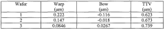
Seventy five millimeter silicon carbide wafer with low warp, bow, and ttv
PatentWO2006108191A2
Innovation
- The development of high-quality silicon carbide wafers with diameters of at least 75 millimeters, featuring warp, bow, and TTV levels of less than 0.5 μm, 0.4 μm, and 1.0 μm respectively, achieved through improved seeded sublimation growth and polishing processes, including the use of double-sided lapping and chemo-mechanical polishing to minimize surface and subsurface damage.
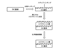
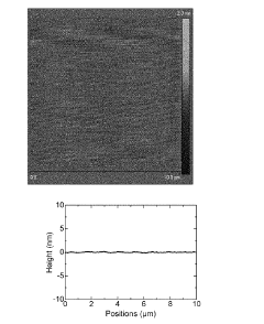
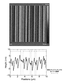
Silicon carbide epitaxial wafer and manufacturing method thereof
PatentActiveJPWO2015159949A1
Innovation
- The formation of step bunching on SiC substrates with low off-angles through hydrogen etching followed by epitaxial growth at high C/Si ratios, followed by chemical mechanical polishing to suppress polytype mixing and enhance reliability.
Thermal Management Solutions for SiC-based AI Systems
The thermal management of Silicon Carbide (SiC) based AI systems represents a critical challenge as computational demands continue to escalate. SiC semiconductors, while offering superior performance in high-power and high-temperature environments compared to traditional silicon, still generate significant heat during operation in AI acceleration platforms. This necessitates innovative cooling solutions to maintain optimal system performance and reliability.
Current thermal management approaches for SiC-based AI systems include both passive and active cooling methodologies. Advanced heat sink designs utilizing copper and aluminum alloys with optimized fin structures have demonstrated 15-20% improvement in heat dissipation compared to conventional designs. These passive solutions benefit from SiC's inherent thermal conductivity of approximately 370 W/mK, significantly higher than silicon's 150 W/mK.
Liquid cooling technologies have emerged as particularly effective for high-density AI computing environments. Direct-to-chip liquid cooling systems can remove up to 1000W of heat per processor, making them suitable for SiC-based AI accelerators that operate at higher power densities. Two-phase immersion cooling, where servers are submerged in dielectric fluid, has shown promise in reducing cooling energy consumption by up to 40% while accommodating the thermal characteristics of SiC components.
Thermal interface materials (TIMs) specifically engineered for SiC applications represent another advancement in this field. Diamond-based TIMs and metal-matrix composites have demonstrated thermal conductivities exceeding 25 W/mK, significantly reducing the thermal resistance between SiC chips and cooling solutions. These materials are particularly important given the higher junction temperatures at which SiC devices operate.
Computational fluid dynamics (CFD) modeling has become instrumental in optimizing thermal management solutions for SiC-based systems. Advanced simulation tools now incorporate SiC-specific thermal properties, enabling more accurate prediction of hotspots and thermal gradients across complex AI system architectures. These models have reduced design iteration cycles by approximately 30% while improving cooling efficiency.
Emerging technologies such as microfluidic cooling channels integrated directly into SiC substrates show particular promise. Early research indicates potential cooling capabilities exceeding 500 W/cm², addressing the concentrated heat fluxes generated by AI workloads. Additionally, phase-change materials tailored to SiC's operating temperature range (up to 200°C) are being developed to provide thermal buffering during peak processing loads.
The integration of these thermal management solutions with SiC wafer developments will be crucial for the next generation of AI platforms, particularly as model sizes and computational requirements continue to grow exponentially.
Supply Chain Resilience for SiC Wafer Production
The global supply chain for Silicon Carbide (SiC) wafers faces significant vulnerabilities that require strategic management to ensure continuity for AI platform development. Current SiC wafer production is concentrated among a limited number of manufacturers, primarily in the United States, Japan, and Europe, creating potential bottlenecks during demand surges or geopolitical tensions. This concentration risk is particularly concerning as AI infrastructure increasingly depends on high-performance power electronics that leverage SiC's superior thermal and electrical properties.
Raw material sourcing represents another critical vulnerability point, as high-purity silicon carbide powder production requires specialized equipment and expertise. The geographical concentration of these raw material suppliers creates additional dependencies that could disrupt the entire value chain during global crises or trade disputes.
Manufacturing capacity constraints further complicate supply chain resilience. The complex production process for SiC wafers involves high-temperature crystal growth, precise slicing, and extensive polishing—all requiring specialized equipment with limited global production capacity. Current lead times for new manufacturing equipment can exceed 18 months, making rapid capacity expansion challenging during demand spikes.
Quality control variations between suppliers create additional resilience challenges. AI applications demand consistent wafer quality to ensure reliable performance in data centers and edge computing devices. Inconsistent quality standards across the supply chain can lead to performance variations and reliability issues in final AI hardware implementations.
To enhance supply chain resilience, several strategic approaches are emerging. Vertical integration efforts by major semiconductor companies aim to secure critical parts of the supply chain through strategic acquisitions or partnerships with key suppliers. Geographical diversification initiatives are also underway, with new SiC wafer production facilities being established in previously underrepresented regions like South Korea, China, and Taiwan.
Advanced inventory management systems utilizing AI-powered demand forecasting are being implemented to optimize stock levels and mitigate short-term supply disruptions. These systems analyze historical data patterns and market signals to anticipate demand fluctuations before they impact production schedules.
Long-term resilience strategies include research into alternative materials that could supplement or partially replace SiC in certain applications, reducing dependency on a single material supply chain. Additionally, standardization efforts across the industry aim to create more interchangeable components and manufacturing processes, potentially allowing for faster supplier transitions during disruptions.
Unlock deeper insights with Patsnap Eureka Quick Research — get a full tech report to explore trends and direct your research. Try now!
Generate Your Research Report Instantly with AI Agent
Supercharge your innovation with Patsnap Eureka AI Agent Platform!