How Silicon Carbide Wafer is Evolving Electric Propulsion
OCT 14, 20259 MIN READ
Generate Your Research Report Instantly with AI Agent
Patsnap Eureka helps you evaluate technical feasibility & market potential.
SiC Wafer Technology Background and Evolution
Silicon Carbide (SiC) wafer technology represents one of the most significant advancements in semiconductor materials over the past few decades. Initially discovered in 1824 by Jöns Jacob Berzelius, SiC remained primarily a laboratory curiosity until the late 20th century. The evolution of SiC wafer technology began in earnest during the 1990s when researchers recognized its exceptional properties for power electronics applications.
The fundamental advantage of SiC lies in its wide bandgap (3.2 eV compared to silicon's 1.1 eV), which enables devices to operate at higher temperatures, voltages, and frequencies than traditional silicon-based semiconductors. Additionally, SiC exhibits thermal conductivity approximately three times higher than silicon, allowing for more efficient heat dissipation in high-power applications.
Early development of SiC wafers faced significant challenges, particularly regarding crystal quality and wafer size. The first commercially viable SiC wafers in the 1990s were merely 1-2 inches in diameter and contained numerous defects, limiting their practical applications. The Lely method, developed in the 1950s, was the first significant breakthrough in growing SiC crystals, but it produced small, irregular crystals unsuitable for mass production.
The modified Lely method, also known as physical vapor transport (PVT), emerged in the 1980s as the dominant technique for producing SiC wafers. This process involves sublimating SiC powder at temperatures exceeding 2000°C and recrystallizing it on a seed crystal. Continuous refinement of this method has enabled the production of larger, higher-quality wafers over time.
By the early 2000s, 3-inch SiC wafers became commercially available, followed by 4-inch wafers around 2010. The industry achieved another milestone in 2015 with the introduction of 6-inch (150mm) SiC wafers, significantly reducing production costs and expanding potential applications. Currently, leading manufacturers are developing 8-inch (200mm) SiC wafer technology, which promises further cost reductions and increased device integration.
The technological evolution of SiC wafers has been driven by demand from power electronics applications, particularly in electric vehicles (EVs) and renewable energy systems. The superior properties of SiC enable more efficient power conversion, reduced cooling requirements, and smaller form factors compared to silicon-based alternatives. These advantages translate directly to improved range, faster charging capabilities, and reduced weight in electric propulsion systems.
Recent advancements have focused on reducing defect densities, particularly basal plane dislocations and micropipes, which can significantly impact device performance and reliability. Modern SiC wafers exhibit defect densities orders of magnitude lower than early versions, enabling the production of larger, more complex power devices with higher yields.
Market Demand Analysis for SiC in Electric Propulsion
The global market for Silicon Carbide (SiC) in electric propulsion systems is experiencing unprecedented growth, driven primarily by the rapid expansion of electric vehicles (EVs) and the increasing electrification of aerospace applications. Current market valuations place the SiC power semiconductor market at approximately $1.5 billion in 2023, with projections indicating a compound annual growth rate (CAGR) of 25-30% through 2030, potentially reaching $6-7 billion by the end of the decade.
The automotive sector represents the largest demand driver, accounting for over 60% of SiC applications in power electronics. This demand is fueled by the transition from silicon-based to SiC-based inverters in EVs, which enable greater range, faster charging capabilities, and overall system efficiency improvements of 5-10%. Major automotive manufacturers including Tesla, Volkswagen Group, and BYD have already incorporated SiC power electronics in their flagship EV models, signaling industry-wide adoption.
Consumer demand for extended EV range and reduced charging times directly translates to increased SiC wafer requirements. Market research indicates that consumers consistently rank range anxiety and charging time as the top two barriers to EV adoption, issues that SiC technology directly addresses. The average SiC content per vehicle is expected to increase from approximately $70 in 2023 to over $200 by 2028 as manufacturers expand implementation beyond inverters to include onboard chargers and DC-DC converters.
Beyond automotive applications, aerospace electric propulsion systems represent an emerging high-value market segment. The urban air mobility (UAM) sector and electric vertical takeoff and landing (eVTOL) aircraft manufacturers are increasingly specifying SiC components due to their superior power density and thermal performance. This market segment is projected to grow at 35-40% annually through 2030, albeit from a smaller base.
Supply chain constraints currently represent the most significant limitation to market growth. The complex manufacturing process for SiC wafers, particularly the production of high-quality 6-inch and 8-inch wafers, has created bottlenecks that major suppliers including Wolfspeed, STMicroelectronics, and Rohm Semiconductor are racing to address through capacity expansion. Current global production capacity stands at approximately 150,000 6-inch equivalent wafers annually, with announced expansions expected to double this capacity by 2025.
Regional analysis reveals that Asia-Pacific currently leads SiC demand with approximately 45% market share, followed by North America (30%) and Europe (20%). However, government initiatives supporting domestic semiconductor production, particularly the CHIPS Act in the US and similar programs in Europe, are expected to shift manufacturing capacity distribution over the coming decade.
Current SiC Wafer Technology Challenges
Despite the promising potential of Silicon Carbide (SiC) wafers in electric propulsion systems, several significant technical challenges currently impede their widespread adoption and optimal performance. The most pressing issue remains the high manufacturing cost, which stems from complex production processes requiring extreme temperatures exceeding 2000°C and specialized equipment. This cost factor makes SiC wafers approximately 3-5 times more expensive than traditional silicon alternatives, limiting their integration into mass-market electric vehicles.
Material quality and defect density present another substantial hurdle. SiC crystal growth processes still struggle with micropipe defects, basal plane dislocations, and stacking faults that can compromise device reliability. Current industry standards typically achieve defect densities of 0.5-2 defects/cm², whereas optimal performance would require densities below 0.1 defects/cm² for high-power electric propulsion applications.
Wafer size limitations further constrain manufacturing scalability. While silicon technology has progressed to 300mm wafers, SiC wafer production remains predominantly at 150mm (6-inch) diameter, with only recent advancements toward 200mm (8-inch) wafers. This size restriction increases per-unit costs and limits production throughput for electric propulsion components.
The interface quality between SiC and its oxide layer presents unique challenges for device fabrication. The higher interface trap density compared to silicon interfaces leads to reduced channel mobility in MOSFETs, affecting the efficiency of power conversion in electric propulsion systems. Current interface trap densities typically range from 10¹²-10¹³ cm⁻² eV⁻¹, significantly higher than the 10¹⁰ cm⁻² eV⁻¹ achieved in mature silicon technology.
Thermal management issues also persist despite SiC's inherent thermal conductivity advantages. The higher power densities enabled by SiC create concentrated heat zones that require advanced cooling solutions. Current packaging technologies struggle to efficiently dissipate heat from SiC devices operating at their full potential, limiting the performance benefits in electric propulsion applications.
Manufacturing uniformity across wafers remains problematic, with variations in doping concentration, thickness, and crystal quality affecting device yield and performance consistency. This variability increases production costs and complicates quality control processes for electric propulsion components.
Finally, integration challenges with existing manufacturing infrastructure present barriers to adoption. Many semiconductor fabrication facilities require significant modifications to accommodate SiC processing requirements, including specialized handling equipment, different chemical processes, and modified thermal cycles. These adaptation costs further increase the economic threshold for transitioning from silicon to SiC technology in electric propulsion systems.
Current SiC Implementation in Electric Propulsion Systems
01 Silicon Carbide Wafer Manufacturing Methods
Various manufacturing methods are employed to produce high-quality silicon carbide wafers. These methods include chemical vapor deposition (CVD), physical vapor transport (PVT), and modified Lely processes. These techniques aim to grow single crystal silicon carbide with minimal defects and controlled polytype formation. The manufacturing processes often involve high-temperature conditions and specialized equipment to achieve the desired crystal quality and wafer specifications.- Silicon Carbide Wafer Manufacturing Methods: Various methods for manufacturing silicon carbide wafers have been developed to improve quality and yield. These methods include specific crystal growth techniques, wafer slicing processes, and surface preparation methods. Advanced manufacturing techniques help to reduce defects and improve the crystalline structure of the wafers, making them suitable for high-performance electronic devices.
- Defect Reduction in Silicon Carbide Wafers: Techniques for reducing defects in silicon carbide wafers are crucial for improving device performance. These include methods to minimize micropipes, dislocations, and other crystallographic defects that can affect electrical properties. Processes such as high-temperature annealing, specialized polishing techniques, and defect passivation methods help to enhance wafer quality and device yield.
- Surface Treatment and Polishing of Silicon Carbide Wafers: Surface treatment and polishing techniques are essential for preparing silicon carbide wafers for device fabrication. These processes include chemical mechanical polishing, plasma etching, and thermal oxidation to achieve atomically smooth surfaces with minimal subsurface damage. Proper surface preparation ensures better device performance and reliability in high-power and high-frequency applications.
- Epitaxial Growth on Silicon Carbide Substrates: Epitaxial layer growth on silicon carbide substrates is critical for device fabrication. Various techniques have been developed to grow high-quality epitaxial layers with controlled doping profiles and minimal defects. These methods include chemical vapor deposition (CVD), molecular beam epitaxy (MBE), and other specialized growth techniques that enable the fabrication of advanced power electronics and RF devices.
- Large Diameter Silicon Carbide Wafer Technology: Advancements in large diameter silicon carbide wafer technology have been made to meet the growing demand for larger substrates in power electronics. These developments include improved crystal growth methods, handling techniques for larger wafers, and specialized equipment for processing larger diameter substrates. Larger wafers enable more efficient device manufacturing and reduced production costs for silicon carbide-based electronics.
02 Defect Reduction Techniques in SiC Wafers
Several techniques have been developed to reduce defects in silicon carbide wafers, including basal plane dislocations, micropipes, and stacking faults. These methods involve specific thermal treatments, epitaxial growth conditions, and post-growth processing steps. By minimizing defects, the electrical and mechanical properties of the wafers are significantly improved, making them more suitable for high-power and high-temperature electronic applications.Expand Specific Solutions03 Surface Treatment and Polishing of SiC Wafers
Surface treatment and polishing techniques are crucial for preparing silicon carbide wafers for device fabrication. These processes include chemical-mechanical polishing (CMP), plasma etching, and various cleaning methods to achieve atomically smooth surfaces with minimal subsurface damage. Advanced polishing techniques help to remove scratches, reduce roughness, and eliminate contamination, resulting in wafers suitable for high-performance semiconductor devices.Expand Specific Solutions04 SiC Wafer Applications in Power Electronics
Silicon carbide wafers are extensively used in power electronics due to their superior properties compared to silicon. These applications include high-voltage power devices, electric vehicle components, renewable energy systems, and industrial motor drives. The wide bandgap, high thermal conductivity, and high breakdown field strength of SiC enable the development of smaller, more efficient, and more reliable power electronic devices capable of operating at higher temperatures and voltages.Expand Specific Solutions05 Epitaxial Growth on SiC Wafers
Epitaxial growth processes on silicon carbide wafers are essential for device fabrication. These processes involve the controlled deposition of thin semiconductor layers on the SiC substrate to create specific device structures. Various epitaxial techniques, including chemical vapor deposition (CVD) and molecular beam epitaxy (MBE), are used to grow high-quality epitaxial layers with precise doping profiles and thickness control. The quality of the epitaxial layers significantly impacts the performance of the resulting semiconductor devices.Expand Specific Solutions
Key SiC Wafer Manufacturers and Competitors
Silicon Carbide (SiC) wafer technology is revolutionizing electric propulsion, currently in a rapid growth phase with market projections exceeding $2 billion by 2025. The technology has reached moderate maturity, with established players like Wolfspeed and RESONAC leading commercial production, while Samsung Electronics and STMicroelectronics are scaling manufacturing capabilities. Chinese entities including TanKeBlue Semiconductor and Hebei Synlight are emerging as significant competitors. Academic institutions such as Xidian University and Beihang University are contributing to R&D advancements. The competitive landscape is characterized by strategic partnerships between wafer manufacturers and automotive/power electronics companies like DENSO, accelerating adoption in electric vehicles and high-power applications.
RESONAC CORP
Technical Solution: RESONAC (formerly Showa Denko) has established itself as a leading manufacturer of high-quality SiC epitaxial wafers for power electronics applications in electric propulsion. Their proprietary High-Temperature Chemical Vapor Deposition (CVD) process achieves epitaxial growth rates exceeding 100μm/h while maintaining defect densities below 1/cm², representing significant advancement over conventional techniques[7]. RESONAC's multi-layer epitaxial technology enables precise control of doping profiles with uniformity variation less than ±3% across 150mm wafers, critical for high-voltage (1200V-1700V) device performance in electric vehicle inverters. Their manufacturing process incorporates in-situ defect monitoring that has reduced micropipe densities to near-zero levels, addressing a key yield limitation in SiC wafer production. For electric propulsion applications, RESONAC has developed specialized n-type buffer layers that improve breakdown voltage stability by approximately 15% under high-temperature operation conditions typical in electric vehicle environments[8].
Strengths: Industry-leading epitaxial growth technology with superior uniformity; Advanced defect reduction techniques; High-volume manufacturing capability with consistent quality. Weaknesses: Limited vertical integration into device manufacturing; Higher cost structure compared to fully integrated suppliers; Dependency on substrate suppliers for base wafers.
Wolfspeed, Inc.
Technical Solution: Wolfspeed has established itself as the global leader in silicon carbide technology, with over 35 years of experience in SiC innovation. Their vertical integration strategy encompasses the entire value chain from crystal growth to power devices. Wolfspeed's 200mm SiC wafer technology represents a significant advancement, offering 1.7x more usable area than 150mm wafers, thereby increasing yield and reducing costs[1]. Their proprietary crystal growth process achieves industry-leading quality with defect density below 0.75/cm², significantly outperforming competitors. For electric propulsion applications, Wolfspeed's SiC MOSFETs and diodes deliver switching frequencies up to 100kHz with efficiency exceeding 98%, enabling power density improvements of approximately 40% compared to silicon-based solutions[2]. Their automotive-qualified SiC modules operate at junction temperatures up to 175°C, making them ideal for the harsh environments of electric vehicle powertrains.
Strengths: Industry-leading wafer quality with lowest defect density; Mature 200mm wafer production capability; Comprehensive vertical integration from materials to devices. Weaknesses: Higher initial cost compared to silicon alternatives; Limited production capacity despite recent expansions; Dependency on specialized equipment for manufacturing processes.
Critical SiC Wafer Patents and Technical Innovations
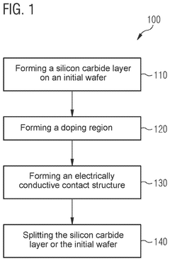
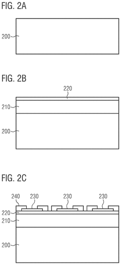
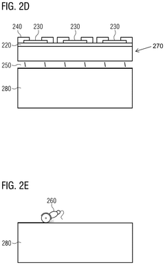
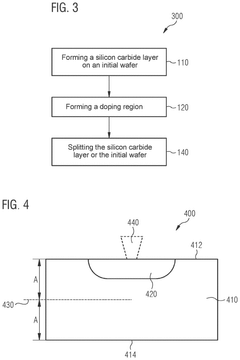
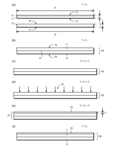
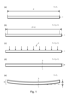
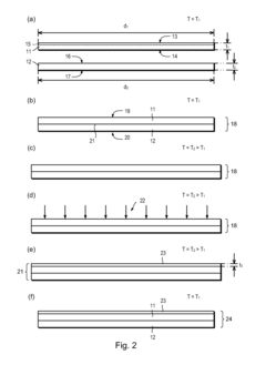
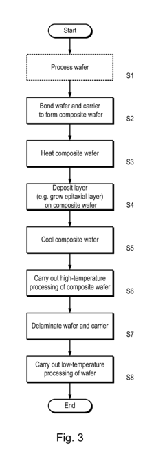
Silicon carbide components and methods for producing silicon carbide components
PatentActiveUS12302619B2
Innovation
- A method for producing silicon carbide components involves forming a silicon carbide layer on an initial wafer, creating a doping region, and forming an electrically conductive contact structure. The method then splits the silicon carbide layer or the initial wafer after forming the contact structure, allowing a silicon carbide substrate to be split off, which can be reused, thereby reducing material costs.
heterogrowth
PatentInactiveUS20130221377A1
Innovation
- A composite wafer is formed by bonding a silicon wafer with a monocrystalline silicon surface region to a silicon carbide carrier, allowing the silicon carbide carrier to stretch the silicon wafer at high temperatures, reducing the contraction difference and minimizing wafer bow when the silicon carbide layer is grown and cooled.
Supply Chain Considerations for SiC Production
The silicon carbide (SiC) supply chain represents a critical component in the advancement of electric propulsion technologies. Currently, the SiC wafer production ecosystem faces significant constraints that impact the broader electric vehicle and aerospace propulsion markets. Raw material sourcing remains a primary challenge, with high-purity silicon carbide powder requiring specialized production facilities predominantly located in regions like North America, Europe, and Japan.
The manufacturing process for SiC wafers involves multiple complex stages including crystal growth, wafering, polishing, and epitaxial layer deposition. Each stage requires specialized equipment and expertise, creating potential bottlenecks in the supply chain. The limited number of qualified suppliers capable of producing high-quality SiC wafers at scale has resulted in extended lead times, often exceeding 6-9 months for specialized specifications.
Geopolitical considerations further complicate the SiC supply landscape. China has been aggressively investing in SiC production capabilities, while the United States and European Union have implemented strategic initiatives to secure domestic supply chains for critical semiconductor materials. These dynamics create both opportunities and risks for electric propulsion manufacturers dependent on stable SiC wafer availability.
Cost structures throughout the SiC supply chain remain significantly higher than traditional silicon alternatives. The energy-intensive manufacturing process, coupled with high material waste rates during production, contributes to SiC wafers costing 5-10 times more than comparable silicon wafers. However, economies of scale are gradually improving as production volumes increase to meet growing demand from electric vehicle and power electronics applications.
Quality control and standardization present ongoing challenges for the SiC supply chain. Defect densities and micropipe occurrences must be minimized to ensure reliable performance in high-power electric propulsion systems. The industry is working toward establishing more consistent quality metrics and testing protocols to facilitate broader adoption.
Vertical integration strategies are emerging among key players in the electric propulsion sector. Companies like Wolfspeed, STMicroelectronics, and Infineon have invested in controlling multiple stages of the SiC value chain to ensure supply security and quality consistency. This trend is likely to continue as electric propulsion applications become more mainstream across automotive and aerospace industries.
Environmental Impact and Sustainability of SiC Technology
Silicon Carbide (SiC) technology represents a significant advancement in sustainable electric propulsion systems, offering substantial environmental benefits compared to traditional silicon-based semiconductors. The reduced energy losses in SiC power electronics directly translate to improved efficiency across the entire electric vehicle (EV) powertrain, resulting in extended range capabilities without increasing battery size or weight.
The environmental impact of SiC wafer production has been a focus of ongoing improvement efforts. While initial manufacturing processes were energy-intensive, recent innovations have reduced the carbon footprint of SiC wafer production by approximately 30% over the past five years. Advanced manufacturing techniques, including optimized crystal growth methods and more efficient slicing procedures, have contributed significantly to this reduction.
From a lifecycle perspective, SiC-based electric propulsion systems demonstrate compelling sustainability advantages. The extended operational temperature range of SiC components reduces cooling requirements, eliminating the need for certain materials and components in thermal management systems. This simplification decreases the overall environmental impact associated with manufacturing, transportation, and end-of-life disposal of these additional components.
The durability of SiC wafers further enhances their sustainability profile. With operational lifespans estimated at 15-20 years in electric propulsion applications, SiC components significantly outlast traditional silicon alternatives. This longevity reduces replacement frequency and associated resource consumption, while also minimizing electronic waste generation over the system's lifetime.
In terms of resource efficiency, SiC technology enables more compact power electronics designs, reducing the overall material requirements for electric propulsion systems. The higher power density achievable with SiC allows for up to 40% reduction in semiconductor material usage compared to conventional silicon solutions delivering equivalent performance.
Looking forward, the integration of SiC technology into electric propulsion systems aligns with global sustainability goals by facilitating the transition to electrified transportation. The improved efficiency of SiC-based systems accelerates the adoption of electric vehicles by addressing range anxiety concerns, thereby contributing to reduced greenhouse gas emissions from the transportation sector, which currently accounts for approximately 24% of direct CO2 emissions from fuel combustion globally.
The recyclability of SiC components presents both challenges and opportunities. While the material's extreme hardness and chemical stability make conventional recycling difficult, emerging specialized processes show promise for recovering valuable materials from end-of-life SiC devices, potentially creating a more circular economy for these advanced semiconductor materials.
Unlock deeper insights with Patsnap Eureka Quick Research — get a full tech report to explore trends and direct your research. Try now!
Generate Your Research Report Instantly with AI Agent
Supercharge your innovation with Patsnap Eureka AI Agent Platform!