Silicon Carbide Wafer in Advanced Telecommunications
OCT 14, 20259 MIN READ
Generate Your Research Report Instantly with AI Agent
Patsnap Eureka helps you evaluate technical feasibility & market potential.
SiC Wafer Technology Background and Objectives
Silicon Carbide (SiC) wafer technology represents a significant advancement in semiconductor materials, evolving from its initial applications in power electronics to becoming increasingly relevant in telecommunications infrastructure. The historical development of SiC began in the early 20th century, but commercial viability only emerged in the 1990s with improved manufacturing techniques. The progression from small-diameter wafers (2-inch) to current 6-inch and emerging 8-inch platforms marks critical milestones in this technology's maturation.
The fundamental advantage of SiC lies in its superior material properties compared to traditional silicon. With a bandgap nearly three times wider than silicon (3.26 eV versus 1.12 eV), SiC enables devices to operate at significantly higher voltages, temperatures, and frequencies. Its thermal conductivity of approximately 370-490 W/m·K far exceeds silicon's 150 W/m·K, allowing for more efficient heat dissipation in high-power applications.
In the telecommunications context, SiC wafers are becoming increasingly critical as networks evolve toward 5G and future 6G technologies. These advanced networks demand higher frequency operations, increased power efficiency, and greater reliability under challenging environmental conditions. The technical objectives for SiC wafer development in telecommunications include achieving higher purity levels with defect densities below 1/cm², larger diameter wafers for economies of scale, and more consistent wafer-to-wafer properties.
Current research focuses on addressing several key challenges: reducing micropipe defects, improving surface quality through advanced polishing techniques, and developing more cost-effective manufacturing processes. The goal is to position SiC as a viable platform for RF components in telecommunications infrastructure, particularly for high-frequency, high-power applications where traditional silicon technology faces fundamental limitations.
The telecommunications industry's transition toward more distributed network architectures, with numerous small cells replacing fewer large base stations, creates new opportunities for SiC technology. These small cells require compact, efficient power amplifiers and other RF components that can operate reliably in various environmental conditions—precisely the strengths of SiC-based devices.
Looking forward, the technical roadmap for SiC in telecommunications aims to achieve 8-inch wafers with defect densities below 0.5/cm² by 2025, enabling a new generation of high-efficiency RF power amplifiers, filters, and switches. These components will be essential for meeting the increasing bandwidth and energy efficiency demands of next-generation telecommunications networks while supporting the industry's sustainability goals through reduced power consumption.
Telecommunications Market Demand Analysis
The telecommunications industry is experiencing a significant transformation driven by the need for higher data transmission speeds, increased bandwidth, and improved energy efficiency. Silicon Carbide (SiC) wafers have emerged as a critical material in this evolution, particularly for advanced telecommunications infrastructure. Market analysis indicates that the global 5G infrastructure market, where SiC components play a crucial role, is projected to grow at a CAGR of 34.2% from 2022 to 2030, reaching a market value of $131.4 billion by 2030.
The demand for SiC wafers in telecommunications is primarily driven by their superior properties compared to traditional silicon, including higher thermal conductivity, wider bandgap, and greater electric field breakdown strength. These characteristics enable the development of high-frequency, high-power devices essential for next-generation telecommunications systems. The market for SiC power semiconductors specifically for telecommunications applications is expected to grow at 25.7% annually through 2027.
Base station infrastructure represents a significant market segment for SiC wafers, with the global market for telecom base stations projected to reach $98.3 billion by 2025. The transition to 5G and future 6G networks requires more base stations with higher power density and efficiency, creating substantial demand for SiC-based power amplifiers and other components. Industry reports indicate that a single 5G base station can consume up to 3.5 times more energy than its 4G counterpart, highlighting the critical need for the energy efficiency that SiC technology provides.
Satellite communications represent another growing market segment for SiC wafers. The global satellite communication market is expected to reach $42.8 billion by 2026, with a CAGR of 9.8%. SiC-based components are increasingly essential in satellite transponders and ground station equipment due to their radiation hardness and reliability in extreme environments.
Data centers supporting telecommunications infrastructure are also driving demand for SiC technology. With global data center power consumption projected to reach 8% of total worldwide electricity by 2030, the energy efficiency benefits of SiC-based power electronics become increasingly valuable. The market for power electronics in data centers is growing at 22.3% annually, with SiC devices capturing an increasing share.
Regional analysis shows that Asia-Pacific currently dominates the market demand for SiC in telecommunications, accounting for approximately 45% of global consumption, followed by North America at 30% and Europe at 20%. China's ambitious 5G rollout plans and investments in telecommunications infrastructure are particularly significant drivers of regional demand growth.
SiC Wafer Development Status and Technical Barriers
Silicon carbide (SiC) wafer technology has reached a critical juncture in its development trajectory, with significant implications for advanced telecommunications systems. Currently, commercial production primarily focuses on 4-inch and 6-inch SiC wafers, while 8-inch wafers remain in the research and development phase. The quality of these wafers has improved substantially over the past decade, with defect densities decreasing from over 10,000/cm² to below 1/cm² in premium substrates.
Despite these advancements, several technical barriers persist in SiC wafer manufacturing. Crystal growth challenges represent the foremost obstacle, as the high-temperature conditions (exceeding 2000°C) required for SiC crystallization create significant thermal management difficulties. The formation of micropipes, dislocations, and stacking faults continues to plague production yields, particularly as manufacturers attempt to scale to larger diameters.
Material purity presents another significant challenge. Nitrogen and boron impurities frequently contaminate SiC crystals during growth, adversely affecting the electrical properties critical for telecommunications applications. Current purification techniques struggle to achieve the ultra-high purity levels (>99.9999%) necessary for next-generation RF and power devices used in 5G and future 6G infrastructure.
Surface finishing represents a third major barrier. The extreme hardness of SiC (9.5 on the Mohs scale) makes traditional polishing techniques inefficient. Chemical-mechanical polishing (CMP) processes for SiC require significant optimization to achieve the sub-nanometer surface roughness essential for advanced device fabrication. Current methods often leave subsurface damage that degrades device performance.
Wafer uniformity across larger diameters remains problematic. As the industry pushes toward 8-inch wafers to improve economics, maintaining consistent crystal quality, thickness, and electrical properties across the entire substrate becomes exponentially more difficult. Edge effects and thermal gradient-induced variations significantly impact device yield in telecommunications applications requiring precise RF characteristics.
Cost factors continue to inhibit widespread adoption. SiC wafers currently cost 5-10 times more than silicon alternatives, primarily due to complex manufacturing processes and lower yields. This price premium restricts SiC's penetration in cost-sensitive telecommunications markets despite its superior technical performance in high-frequency, high-power applications.
Geographically, SiC wafer production capabilities are concentrated in a few regions. The United States, Japan, and Europe lead in high-quality substrate manufacturing, while China has rapidly expanded capacity but struggles with achieving premium quality levels. This concentration creates supply chain vulnerabilities for telecommunications infrastructure development in regions without domestic production capabilities.
Current SiC Solutions for Telecommunications Applications
01 Silicon Carbide Wafer Manufacturing Methods
Various methods for manufacturing silicon carbide wafers have been developed to improve quality and yield. These methods include specific crystal growth techniques, wafer slicing processes, and surface treatment procedures. Advanced manufacturing techniques help to reduce defects and improve the crystalline structure of the wafers, making them suitable for high-performance electronic applications.- Silicon Carbide Wafer Manufacturing Methods: Various methods for manufacturing silicon carbide wafers have been developed to improve quality and yield. These methods include specialized crystal growth techniques, wafer slicing processes, and surface preparation methods. Advanced manufacturing approaches help to reduce defects and improve the crystalline structure of the wafers, making them suitable for high-performance semiconductor applications.
- Defect Reduction in Silicon Carbide Wafers: Techniques for reducing defects in silicon carbide wafers are critical for improving device performance. These include methods for minimizing micropipes, dislocations, and other crystalline imperfections. Processes such as thermal annealing, specialized polishing techniques, and defect passivation help to enhance wafer quality and increase yield in device fabrication.
- Surface Treatment and Polishing of Silicon Carbide Wafers: Surface treatment and polishing methods are essential for preparing silicon carbide wafers for device fabrication. These processes include chemical-mechanical polishing, plasma etching, and other techniques to achieve atomically smooth surfaces with minimal subsurface damage. Proper surface preparation ensures better device performance and reliability in the final semiconductor products.
- Silicon Carbide Epitaxial Growth Techniques: Epitaxial growth techniques for silicon carbide involve depositing thin, high-quality crystalline layers on substrate wafers. These methods include chemical vapor deposition (CVD) and other specialized growth processes that control doping profiles, layer thickness, and crystal quality. Epitaxial layers are crucial for creating the active regions of semiconductor devices with specific electrical properties.
- Large Diameter Silicon Carbide Wafer Production: Advancements in producing larger diameter silicon carbide wafers address the semiconductor industry's need for increased chip yield and reduced manufacturing costs. These developments include modified crystal growth techniques, specialized handling methods, and improved thermal management during processing. Larger wafers enable more efficient production of power devices and other semiconductor components.
02 Defect Reduction in Silicon Carbide Wafers
Techniques for reducing defects in silicon carbide wafers are crucial for improving device performance. These include methods to minimize micropipes, dislocations, and other crystallographic defects that can affect electrical properties. Processes such as high-temperature annealing, specialized polishing techniques, and defect-selective etching help to produce higher quality wafers with fewer imperfections.Expand Specific Solutions03 Surface Treatment and Polishing of Silicon Carbide Wafers
Surface treatment and polishing methods are essential for preparing silicon carbide wafers for device fabrication. These processes include chemical-mechanical polishing, plasma etching, and thermal oxidation to achieve atomically smooth surfaces with minimal subsurface damage. Proper surface preparation ensures better device performance and reliability in the final semiconductor products.Expand Specific Solutions04 Epitaxial Growth on Silicon Carbide Substrates
Epitaxial layer growth on silicon carbide substrates is a critical process for creating functional semiconductor devices. Various techniques have been developed to deposit high-quality epitaxial layers with controlled doping profiles and minimal defects. These methods include chemical vapor deposition (CVD), molecular beam epitaxy (MBE), and other specialized growth processes that enable the fabrication of advanced electronic devices.Expand Specific Solutions05 Large Diameter Silicon Carbide Wafer Technology
Advancements in large diameter silicon carbide wafer technology have been made to meet the increasing demands of the semiconductor industry. These developments include improved crystal growth methods capable of producing larger boules, specialized handling techniques for larger wafers, and adapted processing equipment. Larger diameter wafers enable more efficient device production and lower manufacturing costs per device.Expand Specific Solutions
Key SiC Wafer Manufacturers and Competitive Landscape
The Silicon Carbide (SiC) wafer market in advanced telecommunications is experiencing rapid growth, currently in an early maturity phase with accelerating adoption. The global market is expanding significantly, driven by 5G infrastructure deployment and increasing demand for high-frequency, high-power applications. Technologically, industry leaders like Wolfspeed, Infineon, and STMicroelectronics have established strong positions with commercial-grade SiC wafers, while companies such as TanKeBlue and RESONAC are advancing manufacturing capabilities. Chinese players including BYD and Anhui Weixin Changjiang are increasingly competitive, particularly in domestic markets. Academic-industry collaborations with institutions like University of Warwick and Xidian University are accelerating innovation in wafer quality, size scaling, and defect reduction, positioning SiC as a critical material for next-generation telecommunications infrastructure.
Wolfspeed, Inc.
Technical Solution: Wolfspeed has pioneered silicon carbide (SiC) wafer technology specifically optimized for advanced telecommunications applications. Their 150mm and 200mm SiC wafers feature industry-leading quality with defect densities below 0.5/cm², enabling high-frequency RF power amplifiers with superior thermal conductivity (3-4x higher than silicon). Wolfspeed's proprietary high-purity manufacturing process produces wafers with mobility values exceeding 950 cm²/V·s, critical for 5G and upcoming 6G infrastructure. Their SiC substrates support devices operating at frequencies above 100GHz with power handling capabilities 5-10x greater than GaAs alternatives, while maintaining efficiency above 70% at these frequencies. The company has developed specialized epitaxial growth techniques that enable precise control of doping profiles and layer thicknesses, essential for RF device performance in telecommunications infrastructure.
Strengths: Industry-leading material quality with lowest defect density; Vertical integration from substrate to device manufacturing; Proven reliability in high-frequency telecommunications applications. Weaknesses: Higher production costs compared to silicon alternatives; Limited wafer size options compared to silicon technology; Supply constraints due to high demand across multiple industries.
Infineon Technologies AG
Technical Solution: Infineon has developed advanced SiC wafer technology specifically tailored for telecommunications infrastructure. Their CoolSiC™ platform utilizes 150mm and 200mm SiC wafers with proprietary epitaxial growth processes that achieve carrier mobilities exceeding 900 cm²/V·s and controlled doping profiles within ±5% variation across the wafer. For telecommunications applications, Infineon's SiC wafers support devices operating at breakdown voltages of 650V to 1700V with significantly reduced switching losses (approximately 80% lower than silicon alternatives). Their wafers feature thermal conductivity of approximately 370 W/mK, enabling efficient heat dissipation in densely packed 5G base stations. Infineon has also pioneered specialized surface preparation techniques that improve metal adhesion and reduce interface states, critical for reliable RF performance in telecommunications equipment operating at frequencies up to 80GHz.
Strengths: Comprehensive product portfolio spanning multiple voltage classes; Strong integration with telecommunications system manufacturers; Advanced quality control systems with automotive-grade reliability standards. Weaknesses: Relatively higher cost structure compared to some Asian competitors; Capacity constraints affecting ability to meet rapidly growing demand; Less vertical integration in raw material supply chain compared to some competitors.
Critical Patents and Technical Innovations in SiC Wafers
Silicon carbide single crystal and a method for its production
PatentInactiveUS20050183657A1
Innovation
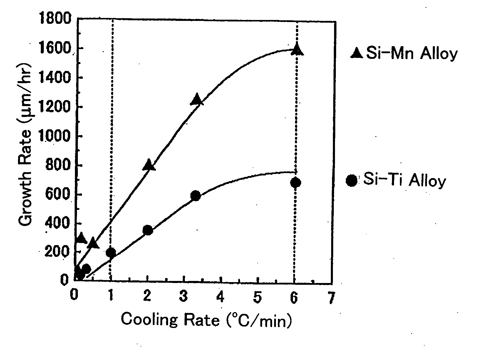
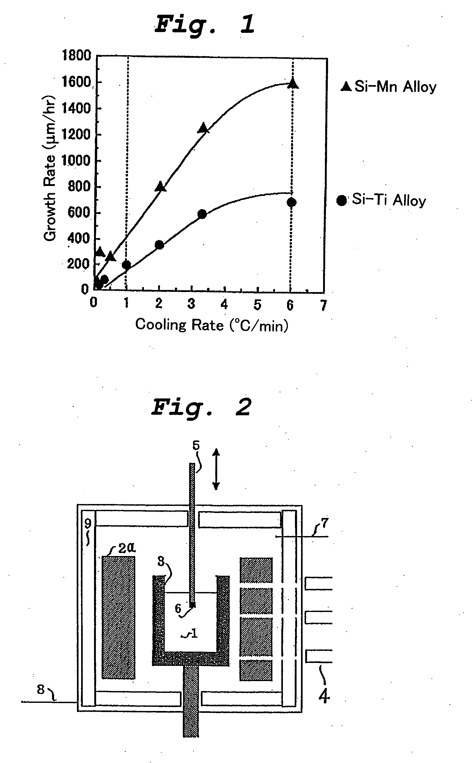
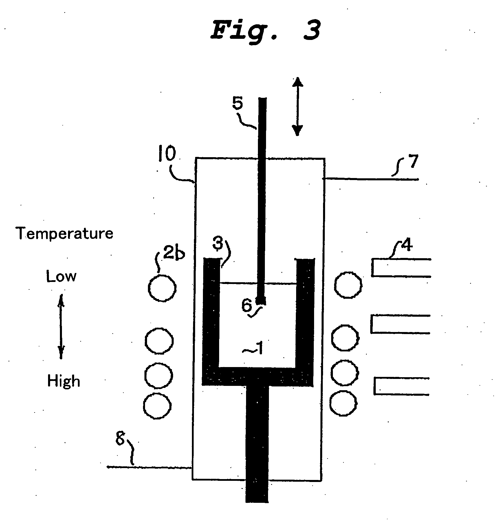
- A method involving immersing a silicon carbide seed substrate in a melt of an Si-C-M alloy with specific atomic ratios of Si and M (Mn or Ti) to create a supersaturated state, allowing for the growth of bulk silicon carbide crystals at temperatures below 2000°C with minimal micropipe defects using either cooling or temperature gradient techniques.
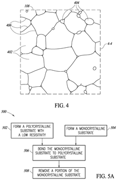
Low resistivity polycrystalline based substrate or wafer
PatentPendingUS20240332365A1
Innovation
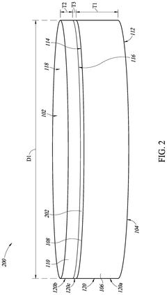
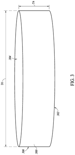
- A polycrystalline silicon carbide wafer with a resistivity of less than or equal to 2 mohm-cm and warpage of less than or equal to 75 μm is developed, coupled with a monocrystalline silicon carbide wafer using surface-activated bonding, reducing on-resistance and mechanical defects.
Supply Chain Resilience and Material Sourcing Strategies
The global supply chain for Silicon Carbide (SiC) wafers faces significant challenges due to limited material sources, complex processing requirements, and increasing demand from telecommunications and other high-tech sectors. Currently, raw SiC material production is concentrated in China, Russia, and parts of Europe, creating geopolitical vulnerabilities for manufacturers in North America and other regions. The COVID-19 pandemic exposed these vulnerabilities when production disruptions led to severe shortages and price volatility in the SiC wafer market, affecting telecommunications infrastructure development.
To address these challenges, leading telecommunications equipment manufacturers are implementing multi-sourcing strategies, establishing relationships with SiC wafer suppliers across different geographical regions. Companies like Ericsson and Nokia have signed long-term supply agreements with multiple vendors to ensure consistent material availability for their 5G and future 6G infrastructure components. These agreements typically include volume commitments and price stabilization mechanisms to protect against market fluctuations.
Vertical integration has emerged as another resilience strategy, with several major players investing in their own SiC production capabilities. Qualcomm and Huawei have made strategic investments in SiC wafer manufacturing facilities, while others have formed joint ventures with established materials companies to secure priority access to high-quality wafers. This approach provides greater control over quality specifications critical for advanced telecommunications applications.
Regional diversification of the supply chain is accelerating, with new SiC production facilities being established in the United States, Japan, and Europe. Government initiatives, such as the CHIPS Act in the US and similar programs in the EU, are providing financial incentives and research support to expand domestic SiC wafer production capacity. These efforts aim to reduce dependency on a limited number of global suppliers and create more resilient regional supply networks.
Innovation in material sourcing is also contributing to supply chain resilience. Research into alternative SiC precursor materials and more efficient synthesis methods is expanding the potential supplier base. Recycling technologies for SiC manufacturing waste are improving yield rates and reducing dependency on virgin materials. Additionally, advanced inventory management systems utilizing AI-driven demand forecasting are helping telecommunications companies optimize their SiC wafer stockpiles without excessive capital commitment.
Collaborative industry initiatives, such as the SiC Consortium and the Telecommunications Material Alliance, are fostering pre-competitive cooperation on supply chain challenges. These groups are developing industry standards for material specifications, qualification processes, and sustainability practices, which help diversify the supplier ecosystem while maintaining quality consistency essential for telecommunications applications.
Environmental Impact and Sustainability Considerations
The production of Silicon Carbide (SiC) wafers for advanced telecommunications presents significant environmental challenges alongside its technological benefits. Manufacturing processes require temperatures exceeding 2000°C, consuming substantial energy and generating considerable carbon emissions. Current production methods typically utilize fossil fuel-powered facilities, contributing to greenhouse gas emissions that contradict global climate goals. Additionally, the chemical vapor deposition (CVD) processes employed in SiC wafer fabrication often involve hazardous gases such as silane and hydrogen chloride, requiring sophisticated containment and disposal systems.
Water usage represents another critical environmental concern, with estimates suggesting that producing a single 6-inch SiC wafer requires between 5,000-8,000 gallons of ultra-pure water. This intensive consumption places pressure on local water resources, particularly in semiconductor manufacturing hubs experiencing water scarcity. Furthermore, the chemical polishing and etching processes generate wastewater containing heavy metals and toxic compounds that demand specialized treatment facilities.
Resource efficiency presents both challenges and opportunities in SiC wafer production. The material utilization rate in current manufacturing processes remains relatively low, with approximately 40-50% of raw silicon carbide material becoming waste during ingot growth and wafer slicing. This inefficiency increases both environmental impact and production costs, driving industry efforts toward improved material recovery systems and optimized manufacturing techniques.
Several sustainability initiatives are emerging across the SiC wafer industry. Leading manufacturers have begun implementing renewable energy sources, with companies like Wolfspeed and STMicroelectronics committing to powering their SiC facilities with solar and wind energy. Closed-loop water recycling systems have demonstrated the potential to reduce freshwater consumption by up to 70%, though implementation remains limited by high capital costs.
End-of-life considerations for SiC-based telecommunications equipment are increasingly important as deployment scales. Unlike traditional silicon, SiC is extremely durable and chemically stable, presenting both advantages and challenges for recycling. While this stability prevents leaching of toxic materials into landfills, it also makes material recovery more difficult. Emerging specialized recycling technologies show promise in recovering valuable materials from SiC devices, potentially creating a circular economy approach that could significantly reduce the environmental footprint of these advanced telecommunications components.
Unlock deeper insights with Patsnap Eureka Quick Research — get a full tech report to explore trends and direct your research. Try now!
Generate Your Research Report Instantly with AI Agent
Supercharge your innovation with Patsnap Eureka AI Agent Platform!