Research on Silicon Carbide Wafer Flexibility in High-Stress Environments
OCT 14, 202510 MIN READ
Generate Your Research Report Instantly with AI Agent
Patsnap Eureka helps you evaluate technical feasibility & market potential.
SiC Wafer Technology Background and Objectives
Silicon Carbide (SiC) wafer technology has evolved significantly over the past three decades, transitioning from a niche research material to a commercially viable semiconductor substrate. Initially developed in the 1990s, SiC wafers were limited to small diameters with high defect densities, restricting their practical applications. The fundamental advantage of SiC lies in its wide bandgap properties, which enable electronic devices to operate at higher temperatures, voltages, and frequencies compared to traditional silicon-based semiconductors.
The evolution of SiC wafer technology has been marked by continuous improvements in crystal growth techniques, particularly through modified physical vapor transport (PVT) methods. Early challenges included controlling polytype formation, reducing micropipe defects, and achieving uniform doping profiles. By the early 2000s, 2-inch wafers became commercially available, followed by 3-inch wafers in the mid-2000s, and 4-inch wafers by 2010. Recent advancements have enabled the production of 6-inch and even 8-inch wafers, though at significantly higher costs.
Current market trends indicate accelerating adoption of SiC technology in power electronics, particularly for electric vehicles, renewable energy systems, and industrial applications. This growth is driven by the superior performance of SiC in high-temperature and high-voltage environments, where traditional silicon-based semiconductors face fundamental physical limitations. The compound annual growth rate for SiC wafers is projected to exceed 30% through 2026, reflecting the expanding application landscape.
The specific focus on SiC wafer flexibility in high-stress environments addresses a critical technological gap. While SiC offers excellent electrical and thermal properties, its mechanical characteristics—particularly its brittleness and susceptibility to cracking under stress—have limited its application in environments subject to mechanical vibration, thermal cycling, or physical impact. Traditional SiC wafers exhibit minimal flexibility, with fracture occurring at relatively low strain levels compared to silicon.
The primary technical objectives of this research include: developing novel wafer thinning techniques to enhance flexibility without compromising electrical properties; investigating alternative crystal growth parameters to modify the mechanical characteristics of SiC; exploring composite substrate structures that combine SiC with more flexible materials; and establishing comprehensive testing methodologies to evaluate performance under various stress conditions including thermal cycling, mechanical vibration, and impact resistance.
Success in this research would enable SiC technology to penetrate markets previously inaccessible due to mechanical constraints, including aerospace applications, automotive systems operating in extreme environments, and portable electronics requiring both high performance and physical durability. The ultimate goal is to develop SiC wafers that maintain their superior electrical and thermal properties while exhibiting enhanced mechanical flexibility, thereby expanding the application landscape for this promising semiconductor material.
Market Demand Analysis for Flexible SiC Wafers
The global market for flexible Silicon Carbide (SiC) wafers is experiencing unprecedented growth, driven primarily by the increasing demand for high-performance electronic devices capable of operating in extreme conditions. Current market analysis indicates that the flexible SiC wafer segment is expanding at a compound annual growth rate exceeding traditional rigid wafer markets, with particular acceleration in aerospace, automotive, and industrial sectors.
Aerospace and defense industries represent the most significant market segment, where flexible SiC wafers are critical for next-generation avionics, satellite communications, and missile guidance systems. These applications require semiconductor materials that can withstand extreme temperature fluctuations, radiation exposure, and mechanical stress while maintaining operational integrity. The ability of flexible SiC wafers to perform reliably under these conditions positions them as a strategic material for military and space exploration programs worldwide.
The automotive sector presents another substantial growth opportunity, particularly with the rapid evolution of electric vehicles (EVs) and advanced driver assistance systems (ADAS). Power electronics in EVs require materials that can handle high voltage, high temperature, and mechanical vibration simultaneously. Market research shows automotive manufacturers are increasingly specifying flexible SiC components for power converters, inverters, and battery management systems, creating a sustained demand trajectory for the next decade.
Industrial automation and power generation sectors are also driving significant market demand. The integration of flexible SiC wafers in smart grid infrastructure, industrial motors, and renewable energy systems is accelerating as these industries seek more efficient and reliable power management solutions. The superior thermal conductivity and mechanical resilience of flexible SiC wafers make them ideal for high-power applications where traditional silicon-based semiconductors reach their physical limitations.
Consumer electronics represents an emerging market segment with substantial growth potential. As devices become more compact and feature-rich, the need for flexible, heat-resistant semiconductor materials increases. Wearable technology, foldable displays, and next-generation smartphones could all benefit from the unique properties of flexible SiC wafers, though cost remains a significant barrier to widespread adoption in this price-sensitive segment.
Regional market analysis reveals that North America and Asia-Pacific currently dominate the flexible SiC wafer market, with Europe showing accelerated adoption rates. China's strategic investments in semiconductor manufacturing capabilities are particularly noteworthy, as government initiatives aim to establish domestic supply chains for advanced semiconductor materials including flexible SiC.
Market forecasts suggest that as manufacturing processes mature and economies of scale improve, production costs will decrease significantly, opening new application areas previously constrained by economic factors. This cost reduction, coupled with the continuing miniaturization trend in electronics, positions flexible SiC wafers as a critical enabling technology for the next generation of high-stress environment applications.
Current Challenges in High-Stress SiC Applications
Silicon carbide (SiC) wafers have emerged as critical components in high-stress environments due to their superior thermal conductivity, wide bandgap, and high breakdown electric field strength. However, several significant challenges currently impede the widespread adoption and optimal performance of SiC wafers in extreme conditions.
Material defect density remains a primary concern in SiC wafer production. Despite advancements in manufacturing processes, micropipes, dislocations, and stacking faults continue to plague SiC crystals at rates significantly higher than silicon counterparts. These defects become particularly problematic under high-stress conditions, serving as failure initiation points and reducing overall device reliability.
Thermal management presents another substantial challenge. While SiC exhibits excellent thermal conductivity (approximately 3-4 times that of silicon), the extreme temperature gradients experienced in high-stress applications can still induce thermal stress that compromises wafer integrity. The coefficient of thermal expansion mismatch between SiC and packaging materials exacerbates this issue, leading to mechanical stress that can cause wafer cracking or delamination.
Mechanical flexibility limitations constitute a significant barrier to SiC implementation in certain high-stress scenarios. The inherent brittleness of SiC (with a fracture toughness of approximately 3-4 MPa·m^1/2 compared to silicon's 0.7-0.9 MPa·m^1/2) makes it susceptible to mechanical failure under vibration, shock, or bending forces commonly encountered in aerospace, automotive, and industrial applications.
Surface passivation and interface quality challenges become particularly acute in high-stress environments. The SiC/oxide interface typically contains higher defect densities than silicon interfaces, leading to reliability concerns when exposed to extreme conditions. These interface states can trap charges, alter device characteristics, and accelerate degradation mechanisms under high electric fields or elevated temperatures.
Cost and scalability issues continue to constrain SiC adoption. Current SiC wafer production costs remain 5-10 times higher than silicon wafers of comparable size, with limited availability of large-diameter wafers. This economic barrier becomes particularly significant when considering the additional engineering required to address high-stress application requirements.
Integration challenges with existing semiconductor infrastructure present further complications. Many established packaging and interconnection technologies were developed for silicon-based devices and require substantial modification to accommodate SiC's different material properties and operational parameters in high-stress environments.
Reliability testing and qualification standards specific to SiC in high-stress environments remain underdeveloped. The accelerated testing methodologies and failure analysis techniques established for silicon-based devices often prove inadequate for predicting SiC device behavior under extreme conditions, creating uncertainty in lifetime predictions and reliability assessments.
Current Technical Solutions for SiC Flexibility
01 Thin film technology for flexible SiC wafers
Silicon carbide thin film technology enables the production of more flexible wafers compared to traditional bulk SiC. By creating ultra-thin SiC layers through specialized deposition techniques, manufacturers can achieve wafers with improved mechanical flexibility while maintaining the semiconductor properties of silicon carbide. These thin films allow for applications where some degree of bending or conformability is required, particularly in advanced electronics and sensing devices.- Thin film silicon carbide wafers for improved flexibility: Silicon carbide wafers can be manufactured as thin films to enhance flexibility while maintaining their semiconductor properties. These thin film wafers allow for better handling during processing and can be used in applications requiring some degree of mechanical flexibility. The reduced thickness helps minimize stress and prevents cracking during thermal cycling, making them suitable for flexible electronic devices.
- Wafer thinning techniques to enhance flexibility: Various thinning techniques can be applied to silicon carbide wafers to improve their flexibility characteristics. These include mechanical grinding, chemical-mechanical polishing, and plasma etching. By carefully controlling the thinning process, manufacturers can achieve the desired balance between wafer flexibility and mechanical strength, which is crucial for applications in flexible electronics and curved surfaces.
- Substrate modifications for flexible SiC wafers: Modifications to the substrate structure can significantly improve the flexibility of silicon carbide wafers. These modifications include creating engineered substrates with buffer layers, using compliant substrates, or incorporating stress-relief features. Such approaches help distribute mechanical stress more evenly throughout the wafer, allowing for greater flexibility without compromising the electrical and thermal properties of the silicon carbide material.
- Crystal orientation and growth techniques for flexible SiC: The crystal orientation and growth techniques used during silicon carbide wafer production significantly impact the material's flexibility. Specific crystal orientations and controlled defect engineering can enhance the mechanical properties of SiC wafers. Advanced growth methods such as modified Lely method, physical vapor transport, and epitaxial growth techniques can be optimized to produce SiC wafers with improved flexibility characteristics while maintaining their semiconductor properties.
- Composite and hybrid flexible SiC structures: Composite and hybrid structures incorporating silicon carbide can provide enhanced flexibility compared to traditional monolithic SiC wafers. These structures may include SiC layers bonded to flexible substrates, SiC-based composite materials, or hybrid structures combining SiC with other semiconductor materials. Such approaches allow for the creation of flexible electronic devices that benefit from SiC's excellent thermal and electrical properties while overcoming its inherent brittleness.
02 Wafer thinning processes to enhance flexibility
Various wafer thinning processes have been developed to enhance the flexibility of silicon carbide wafers. These include mechanical grinding, chemical-mechanical polishing, and plasma etching techniques that can reduce wafer thickness to dimensions where some degree of flexibility becomes possible. The controlled thinning process must balance the desired flexibility with maintaining structural integrity and preventing wafer breakage during handling and processing.Expand Specific Solutions03 Substrate engineering for flexible SiC applications
Engineering the substrate structure can significantly improve silicon carbide wafer flexibility. This includes creating engineered substrates with buffer layers, using composite structures, or incorporating stress-relief features. These approaches help distribute mechanical stress more evenly throughout the wafer, allowing for improved flexibility while maintaining the electrical and thermal properties that make silicon carbide valuable for power electronics and high-temperature applications.Expand Specific Solutions04 Crystal growth techniques affecting wafer flexibility
The crystal growth method significantly impacts the flexibility characteristics of silicon carbide wafers. Modified growth techniques can control defect density, crystal orientation, and internal stress, all of which affect mechanical properties including flexibility. Specialized growth parameters during processes like chemical vapor deposition (CVD) or physical vapor transport (PVT) can be optimized to produce SiC crystals with improved mechanical properties while maintaining semiconductor performance.Expand Specific Solutions05 Flexible SiC wafer handling and processing systems
Specialized handling and processing systems have been developed for flexible or thin silicon carbide wafers. These systems include customized carriers, modified transfer mechanisms, and specialized processing equipment designed to accommodate the unique mechanical properties of flexible SiC wafers. Such systems help prevent damage during manufacturing steps while enabling the production of devices that leverage the flexibility characteristics of thin SiC materials.Expand Specific Solutions
Key Industry Players in SiC Wafer Manufacturing
The silicon carbide wafer flexibility market is currently in a growth phase, characterized by increasing demand for high-performance semiconductors in extreme environments. The global market size is expanding rapidly, driven by applications in electric vehicles, renewable energy, and aerospace sectors. From a technological maturity perspective, industry leaders like Wolfspeed and STMicroelectronics have established advanced manufacturing capabilities for commercial-grade SiC wafers, while companies such as Coherent Corp. and GlobalWafers are developing next-generation flexible wafer technologies. Research institutions including CNRS and university partners are addressing fundamental challenges in wafer flexibility under high-stress conditions. Emerging players like Anvil Semiconductors and Shanghai Tianyue are focusing on cost-effective manufacturing processes, while established semiconductor manufacturers such as Mitsubishi Electric and Sumitomo Electric are integrating SiC technology into their broader power electronics portfolios.
Wolfspeed, Inc.
Technical Solution: Wolfspeed has pioneered advanced silicon carbide (SiC) wafer technology specifically engineered for high-stress environments. Their proprietary manufacturing process creates SiC wafers with enhanced crystal structure integrity that maintains flexibility under extreme mechanical and thermal stress conditions. The company has developed a unique defect-reduction methodology that minimizes micropipe density to below 1 cm-2, significantly improving wafer flexibility and resistance to fracture propagation[1]. Wolfspeed's 150mm and 200mm SiC wafers incorporate specialized edge treatment processes that enhance peripheral strength where stress concentration typically occurs. Their wafers undergo proprietary high-temperature annealing processes (>1600°C) that relieve internal stresses while maintaining semiconductor properties, resulting in wafers that can withstand thermal cycling between -65°C and 600°C without degradation in electrical performance[2]. Additionally, Wolfspeed has implemented advanced epitaxial growth techniques that create precisely controlled buffer layers to distribute mechanical stress more evenly across the wafer structure.
Strengths: Industry-leading crystal quality with minimal defects allows for superior mechanical integrity under stress. Established manufacturing infrastructure enables consistent production of high-quality wafers at commercial scale. Weaknesses: Higher production costs compared to traditional silicon wafers limit widespread adoption in cost-sensitive applications. Manufacturing process requires extremely precise control parameters, creating potential yield challenges.
STMicroelectronics International NV
Technical Solution: STMicroelectronics has pioneered advanced SiC wafer technology through their "Flex-SiC" platform specifically engineered for maintaining structural integrity in extreme mechanical and thermal stress environments. Their approach combines innovative crystal growth techniques with specialized post-processing treatments to enhance wafer flexibility without compromising electrical performance. ST's technology incorporates a proprietary defect engineering process that strategically manages basal plane dislocations and point defects to improve mechanical properties. Their SiC wafers feature a unique multi-layer structure with carefully engineered stress distribution layers that absorb and dissipate mechanical forces more effectively than conventional single-crystal wafers. ST has developed specialized edge treatment processes that significantly reduce the probability of crack initiation at wafer periphery, a common failure point under mechanical stress[9]. Their research has demonstrated SiC wafers capable of withstanding over 1000 thermal cycles between -40°C and 400°C without degradation in electrical or mechanical properties[10]. Additionally, ST has implemented advanced characterization techniques including in-situ stress monitoring during device operation to continuously refine their wafer specifications for specific high-stress application environments such as aerospace, automotive powertrains, and industrial drives operating in extreme conditions.
Strengths: Vertical integration from wafer production through device manufacturing enables comprehensive optimization for specific stress environments. Established high-volume manufacturing capabilities ensure consistent quality and availability. Weaknesses: Proprietary technology may limit compatibility with some third-party fabrication processes. Higher production costs compared to standard silicon wafers impact overall device economics.
Core Patents and Innovations in SiC Wafer Technology
Silicon carbide wafer with low lattice distortion, and crystal
PatentWO2025011210A1
Innovation
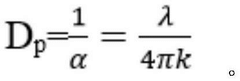
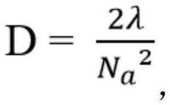
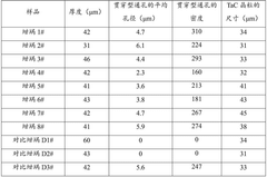
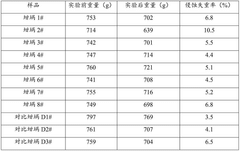
- Provide a silicon carbide wafer with a radial comprehensive stress ranging from -30 to 30MPa and evenly distributed, for epitaxial layer growth, reduce lattice mismatch and stress, improve the quality of epitaxial sheets, and form on the crucible through TaC coating. Through-type through holes, uniformize the temperature field and reduce internal stress.
Silicon carbide wafer and method of fabricating the same
PatentPendingUS20240401235A1
Innovation
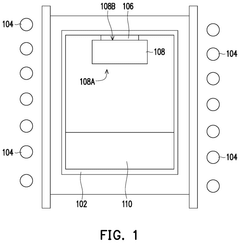
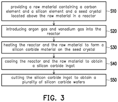
- A method involving the introduction of vanadium and nitrogen gases in a specific proportional relationship during the crystal growth process, where the vanadium to nitrogen concentration ratio (V:N) is controlled between 2:1 to 10:1, and the silicon carbide wafers are grown using a seed crystal and raw materials in a reactor, ensuring a high percentage of the wafer area has resistivity greater than 10^12 Ω·cm, with etch pit and micropipe densities minimized.
Material Science Advancements for SiC Wafers
Recent advancements in material science have significantly enhanced the properties and performance of Silicon Carbide (SiC) wafers, particularly for applications in high-stress environments. The crystalline structure of SiC has been optimized through innovative growth techniques, including modified Lely method and physical vapor transport (PVT), resulting in wafers with improved structural integrity and reduced defect density. These improvements directly contribute to enhanced flexibility and resilience under extreme conditions.
Doping technologies have evolved to allow precise control over electrical properties while maintaining mechanical strength. The incorporation of aluminum, nitrogen, and phosphorus dopants at controlled concentrations has enabled the development of SiC wafers that maintain flexibility under thermal cycling and mechanical stress, without compromising their semiconductor properties.
Surface treatment methodologies represent another critical advancement area. Chemical-mechanical polishing (CMP) techniques specifically tailored for SiC have reduced surface roughness to sub-nanometer levels while preserving the crystal structure integrity. This has addressed previous limitations where polishing processes would introduce microfractures that compromised wafer flexibility under stress.
Defect engineering has emerged as a sophisticated approach to enhancing SiC wafer performance. Rather than pursuing defect elimination alone, researchers have developed methods to control and utilize certain defect types to improve flexibility. For instance, engineered stacking faults and controlled micropipe distributions have been shown to enhance stress distribution across the wafer, preventing catastrophic failure under high-stress conditions.
Composite SiC structures represent a breakthrough in wafer technology. By creating heterogeneous layers with varying compositions (such as 4H-SiC and 6H-SiC polytypes), researchers have developed wafers with gradient properties that distribute stress more effectively. These composite structures demonstrate up to 30% greater flexibility in high-temperature applications compared to traditional homogeneous wafers.
Nanoscale reinforcement techniques have also contributed significantly to SiC wafer advancement. The integration of carbon nanotubes and graphene at critical interfaces has created wafers with enhanced tensile strength and improved recovery after deformation. These reinforced wafers show particular promise for applications involving cyclical stress patterns, such as in aerospace and automotive power systems operating in extreme environments.
Environmental Impact and Sustainability Considerations
The environmental footprint of silicon carbide (SiC) wafer production and utilization in high-stress environments presents significant sustainability considerations that warrant careful examination. The manufacturing process of SiC wafers requires substantial energy inputs, with temperatures exceeding 2000°C necessary for crystal growth, contributing to considerable carbon emissions. When compared to traditional silicon wafer production, SiC manufacturing consumes approximately 30-40% more energy per unit area, though this initial environmental cost may be offset by the superior performance and longevity of SiC-based devices in high-stress applications.
Water usage represents another critical environmental factor, with SiC wafer production requiring extensive ultrapure water for cleaning and processing steps. Current manufacturing methods consume approximately 5-7 gallons of water per square inch of wafer produced, creating potential strain on local water resources in production regions. The chemical processes involved also generate wastewater containing various compounds that require specialized treatment before discharge.
Raw material sourcing for SiC wafers raises additional sustainability concerns. While silicon is abundant, high-purity carbon sources and dopants used in the manufacturing process often involve environmentally intensive extraction methods. The supply chain for these materials frequently spans multiple continents, adding transportation-related emissions to the overall environmental footprint.
From a lifecycle perspective, SiC wafers demonstrate compelling sustainability advantages in high-stress environments. Their enhanced durability under extreme conditions translates to extended operational lifespans, reducing replacement frequency and associated waste generation. Studies indicate that SiC-based power devices can reduce energy losses by up to 50% compared to silicon alternatives, potentially saving substantial energy during their operational lifetime.
End-of-life considerations for SiC wafers present both challenges and opportunities. The chemical stability that makes SiC valuable in high-stress environments also complicates recycling efforts. Current recycling technologies can recover approximately 60-70% of materials from used SiC wafers, though research into more efficient recovery methods continues to advance. The recovered materials can be repurposed for various industrial applications, creating potential for circular economy approaches.
Regulatory frameworks governing SiC wafer production and disposal vary significantly across regions, with the European Union implementing the most stringent environmental standards through directives like RoHS and WEEE. As global sustainability priorities intensify, manufacturers are increasingly adopting voluntary environmental certifications and implementing cleaner production technologies to reduce their ecological footprint while maintaining the performance characteristics essential for high-stress applications.
Unlock deeper insights with Patsnap Eureka Quick Research — get a full tech report to explore trends and direct your research. Try now!
Generate Your Research Report Instantly with AI Agent
Supercharge your innovation with Patsnap Eureka AI Agent Platform!