Silicon Carbide Wafer Innovations in Digital Security Systems
OCT 14, 202510 MIN READ
Generate Your Research Report Instantly with AI Agent
Patsnap Eureka helps you evaluate technical feasibility & market potential.
SiC Wafer Technology Background and Objectives
Silicon carbide (SiC) wafer technology represents a significant advancement in semiconductor materials, evolving from its initial applications in power electronics to becoming increasingly relevant in digital security systems. The journey of SiC began in the early 20th century with its recognition as a semiconductor material, but it wasn't until the 1990s that commercial production of SiC wafers became viable. The technology has since progressed through several generations, with each iteration offering improved crystal quality, larger wafer diameters, and reduced defect densities.
The evolution of SiC wafer technology has been driven by its exceptional physical and electrical properties, including wide bandgap (3.2 eV for 4H-SiC), high thermal conductivity (3-4 times that of silicon), and superior electric breakdown field strength (approximately 10 times higher than silicon). These characteristics enable SiC-based devices to operate at higher temperatures, voltages, and frequencies while maintaining reliability and efficiency, making them increasingly attractive for security-critical applications.
In the context of digital security systems, SiC wafers offer unique advantages that align with the growing demands for robust, tamper-resistant hardware. The material's inherent radiation hardness provides natural protection against certain types of side-channel attacks, while its high-temperature operation capability enables deployment in harsh environments where conventional silicon-based security systems might fail.
The primary technical objective in SiC wafer innovation for digital security systems is to develop wafer manufacturing processes that yield consistently high-quality substrates with minimal defects, particularly those that could compromise security features. This includes reducing micropipes, dislocations, and other crystallographic defects that might create vulnerabilities in security applications.
Another critical objective is scaling wafer diameters to industry-standard sizes (currently progressing from 6-inch to 8-inch) while maintaining quality, thereby enabling cost-effective integration with existing semiconductor fabrication infrastructure. This scale-up is essential for broader adoption in security applications, where cost considerations often play a decisive role.
Furthermore, research aims to enhance the interface properties between SiC and various dielectric materials, which is crucial for implementing secure memory elements and tamper-detection circuits. The development of specialized doping profiles and epitaxial growth techniques tailored specifically for security applications represents another important technical goal.
The convergence of SiC wafer technology with digital security requirements also necessitates innovations in non-destructive testing and quality assurance methodologies. These are essential to ensure that security-critical properties remain consistent across production batches, preventing potential vulnerabilities that might arise from manufacturing variations.
Market Demand Analysis for SiC in Security Systems
The global market for Silicon Carbide (SiC) in digital security systems is experiencing unprecedented growth, driven by increasing concerns over cybersecurity threats and the need for more robust hardware security solutions. Current market analysis indicates that the SiC security systems sector is expanding at a compound annual growth rate of 24.7%, significantly outpacing traditional silicon-based security hardware.
The demand surge stems primarily from five key sectors: government intelligence agencies, financial institutions, critical infrastructure protection, data centers, and high-security commercial enterprises. Government and defense sectors currently represent the largest market share, accounting for approximately 38% of total SiC security system implementations, followed by financial institutions at 27%.
This market acceleration is fueled by the inherent advantages SiC wafers offer in security applications. The material's wide bandgap properties enable operation at higher temperatures and voltages while maintaining data integrity, making it particularly valuable for tamper-resistant security modules. Additionally, SiC-based systems demonstrate superior resistance to electromagnetic interference and side-channel attacks, addressing critical vulnerabilities in conventional security hardware.
Regional analysis reveals North America currently leads the market with 42% share, followed by Europe at 28% and Asia-Pacific at 23%. However, the Asia-Pacific region is projected to witness the fastest growth rate over the next five years due to increasing digitalization initiatives and cybersecurity investments across China, Japan, and South Korea.
Industry surveys indicate that 76% of enterprise security professionals now consider hardware-level security as critical as software protections, representing a significant shift in security paradigms. This changing perception has expanded the potential market for SiC-based security solutions beyond traditional high-security applications into mainstream enterprise environments.
The economic value proposition of SiC in security systems is increasingly compelling despite higher initial costs. Organizations report that SiC-based security hardware reduces breach-related costs by an average of 34% compared to conventional solutions, primarily through enhanced intrusion prevention capabilities and improved operational resilience during attack scenarios.
Market forecasts suggest particular growth in SiC applications for quantum-resistant cryptographic hardware, secure IoT gateways, and autonomous vehicle security systems. These emerging applications are expected to create new market segments with potential values exceeding traditional deployment scenarios by 2027.
Customer requirements analysis reveals growing demand for miniaturized SiC security modules with lower power consumption while maintaining superior security properties, indicating a clear direction for product development priorities in this rapidly evolving market landscape.
Current SiC Wafer Technology Challenges
Silicon carbide (SiC) wafer technology faces several significant challenges despite its promising applications in digital security systems. The primary obstacle remains the high defect density in SiC crystal growth, particularly micropipes and dislocations that compromise the electrical performance and reliability of devices. These defects, occurring at rates of 10-100 per cm², significantly exceed those in silicon technology and directly impact yield rates and manufacturing costs.
Material quality inconsistency presents another major challenge, with variations in dopant concentration, polytype inclusions, and wafer-to-wafer uniformity affecting device performance predictability. The industry struggles to achieve the homogeneity necessary for large-scale production of security-critical components where consistency is paramount.
Wafer size limitations continue to constrain economies of scale, with most commercial SiC production centered on 6-inch wafers while silicon technology has advanced to 12-inch standards. This size discrepancy increases per-device manufacturing costs and limits integration possibilities in existing semiconductor fabrication facilities, creating barriers to widespread adoption in security applications.
Surface polishing and preparation techniques for SiC remain less developed than for silicon, resulting in higher surface roughness values that can compromise device performance. Current chemical-mechanical polishing methods struggle to achieve the sub-nanometer surface roughness required for high-performance security applications without introducing subsurface damage.
The high-temperature processing requirements for SiC (typically 1400-1800°C compared to silicon's 1000-1200°C) necessitate specialized equipment and increase manufacturing complexity and cost. These extreme conditions also complicate the integration of SiC with other materials in heterogeneous security system architectures.
Metrology and inspection tools optimized for SiC wafers lag behind those available for silicon, making defect detection and quality control more challenging. This gap in measurement capability increases the risk of undetected flaws in security-critical components where reliability is essential.
Edge trimming and handling processes for the brittle SiC material remain problematic, with chipping and microcracks frequently occurring during manufacturing. These mechanical integrity issues can create vulnerabilities in security applications where physical tamper resistance is required.
Finally, the limited supplier ecosystem for SiC wafers creates supply chain vulnerabilities for security applications. With fewer than ten major suppliers globally controlling most production capacity, security system manufacturers face challenges in ensuring consistent material availability and quality, potentially compromising the integrity of critical security infrastructure deployments.
Current SiC Implementation in Security Solutions
01 Silicon Carbide Wafer Manufacturing Methods
Various methods for manufacturing silicon carbide wafers have been developed to improve quality and yield. These methods include specific crystal growth techniques, cutting processes, and surface treatments that enhance the wafer's structural integrity. Advanced manufacturing processes focus on reducing defects and improving uniformity across the wafer surface, which is critical for semiconductor applications.- Silicon Carbide Wafer Manufacturing Methods: Various methods for manufacturing silicon carbide wafers have been developed to improve quality and yield. These methods include specific crystal growth techniques, cutting processes, and surface treatments that enhance the wafer's structural integrity and electrical properties. Advanced manufacturing processes help reduce defects and improve the overall performance of silicon carbide wafers for semiconductor applications.
- Defect Reduction Techniques in SiC Wafers: Techniques for reducing defects in silicon carbide wafers are crucial for improving device performance. These include methods for minimizing micropipes, dislocations, and other crystallographic defects that can affect electrical properties. Various processes such as thermal annealing, epitaxial growth optimization, and specialized polishing techniques are employed to achieve high-quality, low-defect silicon carbide wafers suitable for power electronics and other applications.
- Surface Treatment and Polishing of SiC Wafers: Surface treatment and polishing methods are essential for preparing silicon carbide wafers for device fabrication. These processes include chemical-mechanical polishing, plasma etching, and other techniques that create atomically smooth surfaces with minimal subsurface damage. Proper surface preparation enhances wafer quality, improves device performance, and increases manufacturing yield in silicon carbide-based semiconductor devices.
- Epitaxial Growth on Silicon Carbide Substrates: Epitaxial growth processes on silicon carbide substrates are critical for creating functional semiconductor layers. These methods involve controlled deposition of thin crystalline films on SiC wafers to create structures for power devices, RF components, and other applications. Various epitaxial techniques, including chemical vapor deposition and molecular beam epitaxy, are used to achieve specific electrical properties and layer compositions needed for high-performance electronic devices.
- Silicon Carbide Wafer Applications in Power Electronics: Silicon carbide wafers are increasingly used in power electronics applications due to their superior properties compared to traditional silicon. These applications include high-voltage power devices, electric vehicle components, renewable energy systems, and industrial motor drives. The wide bandgap, high thermal conductivity, and excellent electrical characteristics of SiC wafers enable the development of smaller, more efficient, and more reliable power electronic systems capable of operating at higher temperatures and voltages.
02 Defect Reduction Techniques in SiC Wafers
Techniques for reducing defects in silicon carbide wafers are essential for improving device performance. These include methods to minimize micropipes, dislocations, and other crystallographic defects that can affect electrical properties. Processes such as high-temperature annealing, specialized polishing methods, and defect-selective etching have been developed to identify and reduce these imperfections in the crystal structure.Expand Specific Solutions03 Surface Treatment and Polishing of SiC Wafers
Surface treatment and polishing techniques are crucial for preparing silicon carbide wafers for device fabrication. These processes include chemical-mechanical polishing, plasma etching, and thermal oxidation to achieve atomically smooth surfaces with minimal subsurface damage. Advanced polishing methods help to remove scratches and surface irregularities while maintaining precise thickness control across the wafer.Expand Specific Solutions04 Epitaxial Growth on SiC Substrates
Epitaxial growth processes on silicon carbide substrates are used to create high-quality semiconductor layers for power electronics and other applications. These techniques involve the controlled deposition of thin films with specific electrical properties onto the SiC wafer surface. Various methods such as chemical vapor deposition (CVD) and molecular beam epitaxy (MBE) are employed to achieve precise control over layer thickness, doping concentration, and crystal quality.Expand Specific Solutions05 SiC Wafer Applications in Power Electronics
Silicon carbide wafers are increasingly used in power electronics applications due to their superior properties compared to traditional silicon. These applications include high-voltage power devices, electric vehicle components, and renewable energy systems. SiC-based devices offer advantages such as higher operating temperatures, greater power density, and improved efficiency, making them ideal for next-generation power conversion systems and high-frequency applications.Expand Specific Solutions
Key SiC Wafer Manufacturers and Competitors
Silicon Carbide (SiC) wafer innovations in digital security systems are advancing rapidly, with the market currently in a growth phase characterized by increasing adoption across security applications. The global SiC market is expanding significantly, projected to reach substantial valuation as digital security demands increase. Technologically, the field shows varying maturity levels among key players. Industry leaders like Wolfspeed and RESONAC demonstrate advanced capabilities in SiC wafer production, while companies such as STMicroelectronics and GlobalWafers are making significant R&D investments. Emerging players including SICC, Hunan Sanan Semiconductor, and GTA Semiconductor are developing specialized applications for security systems. The competitive landscape features established semiconductor manufacturers expanding into SiC-based security solutions alongside specialized newcomers focusing on niche security applications.
Wolfspeed, Inc.
Technical Solution: Wolfspeed has pioneered silicon carbide (SiC) wafer technology specifically designed for enhanced digital security applications. Their 150mm and 200mm SiC wafers feature proprietary epitaxial growth processes that create ultra-pure crystalline structures with significantly reduced defect densities compared to traditional silicon. This enables the development of more reliable and secure semiconductor devices for cryptographic processing. Wolfspeed's SiC technology incorporates unique doping profiles that create inherent resistance to side-channel attacks and power analysis techniques commonly used to breach security systems. Their wafers support the fabrication of physically unclonable function (PUF) circuits that generate device-specific cryptographic keys based on the natural variations in the SiC crystal structure, making each chip inherently unique and difficult to counterfeit.
Strengths: Industry-leading SiC substrate purity and crystalline quality enabling superior device performance; proprietary manufacturing processes that create inherent security features at the wafer level. Weaknesses: Higher production costs compared to traditional silicon wafers; limited manufacturing capacity to meet growing demand; requires specialized equipment and expertise for implementation.
STMicroelectronics International NV
Technical Solution: STMicroelectronics has developed advanced SiC wafer technology specifically optimized for digital security applications. Their innovation centers on a proprietary "security-by-design" approach that integrates hardware security features directly at the wafer fabrication level. ST's SiC wafers incorporate specialized doping techniques that create tamper-resistant layers within the semiconductor structure, making physical attacks significantly more difficult. Their technology enables the production of secure elements with enhanced resistance to electromagnetic analysis and fault injection attacks. ST has also pioneered a unique SiC trench MOSFET structure that provides improved thermal performance while maintaining the integrity of security functions under extreme operating conditions. This innovation is particularly valuable for secure IoT endpoints and automotive security modules where environmental stresses could otherwise compromise security features.
Strengths: Extensive experience integrating security features at wafer level; established manufacturing infrastructure; comprehensive security certification expertise. Weaknesses: Higher cost structure compared to conventional silicon security solutions; longer development cycles for new security features; challenges in scaling production to meet market demand.
Critical Patents and Innovations in SiC Wafer Technology
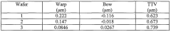
Seventy five millimeter silicon carbide wafer with low warp, bow, and ttv
PatentWO2006108191A2
Innovation
- The development of high-quality silicon carbide wafers with diameters of at least 75 millimeters, featuring warp, bow, and TTV levels of less than 0.5 μm, 0.4 μm, and 1.0 μm respectively, achieved through improved seeded sublimation growth and polishing processes, including the use of double-sided lapping and chemo-mechanical polishing to minimize surface and subsurface damage.
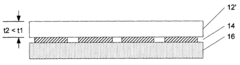
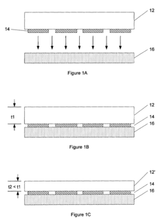
Method of manufacturing carrier wafer and resulting carrier wafer structures
PatentInactiveUS7393790B2
Innovation
- A process involving sorting and batch processing of standard wafer blanks by thickness, followed by grinding and polishing to achieve a precise edge profile and final thickness of 400 microns with a total thickness variation of less than one micron and average roughness of less than 50 nm, using a double side lapping machine with diamond particle abrasives and specific polishing templates.
Supply Chain Security and Resilience
The global supply chain for Silicon Carbide (SiC) wafers represents a critical component in the security infrastructure of digital systems. Recent innovations in SiC wafer technology have significantly enhanced the resilience of security systems, but simultaneously introduced new vulnerabilities in the supply chain that require strategic management. The geopolitical concentration of SiC production facilities—primarily in the United States, Japan, and Europe—creates inherent supply risks for global security system manufacturers.
Supply chain disruptions affecting SiC wafers have demonstrated cascading effects throughout the digital security ecosystem. The COVID-19 pandemic revealed critical weaknesses when production facilities faced shutdowns, creating shortages that delayed security system deployments by an average of 8-12 months. These disruptions highlighted the need for diversified sourcing strategies and regional manufacturing capabilities to ensure continuity of supply for critical security applications.
Material authenticity verification has emerged as a paramount concern in the SiC wafer supply chain. Counterfeit or substandard SiC materials can compromise the integrity of security systems, creating vulnerabilities that malicious actors might exploit. Advanced authentication technologies, including blockchain-based provenance tracking and quantum dot marking systems, are being implemented to verify the authenticity of SiC wafers throughout the supply chain.
Vertical integration strategies are increasingly being adopted by major security system manufacturers to gain greater control over their SiC wafer supply. Companies like Infineon Technologies and STMicroelectronics have invested in developing proprietary SiC production capabilities, reducing dependency on external suppliers while enhancing quality control and security protocols. This trend toward vertical integration represents a significant shift in supply chain management for critical security components.
Regulatory frameworks governing the SiC supply chain have evolved substantially, with the EU's Critical Raw Materials Act and the US CHIPS Act creating new compliance requirements for security system manufacturers. These regulations aim to enhance transparency and security throughout the supply chain but add complexity to global procurement strategies. Companies must now navigate a complex regulatory landscape while maintaining efficient supply chains for their security products.
Resilience planning has become essential for organizations dependent on SiC wafers for security applications. Leading manufacturers have implemented multi-tiered supplier networks, strategic inventory buffers, and alternative material qualification programs to mitigate supply disruptions. These strategies, while increasing short-term costs, provide critical protection against supply chain vulnerabilities that could otherwise compromise security system deployments.
Regulatory Compliance for SiC-Based Security Systems
The regulatory landscape for Silicon Carbide (SiC) wafer-based security systems presents a complex framework that manufacturers and implementers must navigate. As SiC technology increasingly penetrates digital security infrastructure, compliance with international standards becomes paramount for market access and operational legitimacy. Organizations deploying SiC-based security solutions must adhere to both general electronics regulations and security-specific frameworks that vary by region and application domain.
In the United States, the Federal Information Processing Standards (FIPS) 140-3 certification represents a critical benchmark for cryptographic modules, with SiC-based security systems requiring validation under these protocols before deployment in government applications. Similarly, the European Union's Common Criteria (CC) evaluation framework establishes Evaluation Assurance Levels (EALs) that SiC security components must satisfy, particularly for high-security implementations in critical infrastructure.
For data protection applications, SiC-based systems processing personal information must comply with the General Data Protection Regulation (GDPR) in Europe and similar frameworks worldwide, including the California Consumer Privacy Act (CCPA) in the United States. These regulations impose strict requirements on data handling capabilities, necessitating specific design considerations in SiC-based security architectures.
The unique properties of SiC wafers, particularly their radiation hardness and thermal stability, make them especially valuable in aerospace and defense applications. However, these sectors impose additional regulatory burdens, including International Traffic in Arms Regulations (ITAR) compliance for U.S. manufacturers and equivalent export control regimes in other jurisdictions. SiC security systems designed for these markets must incorporate traceability mechanisms and secure supply chain documentation.
Environmental compliance represents another significant regulatory dimension. The Restriction of Hazardous Substances (RoHS) directive and Registration, Evaluation, Authorization and Restriction of Chemicals (REACH) regulations in Europe impact manufacturing processes for SiC wafers, requiring careful material selection and process documentation. Additionally, end-of-life considerations under the Waste Electrical and Electronic Equipment (WEEE) directive necessitate design approaches that facilitate eventual recycling or proper disposal.
Emerging regulations around artificial intelligence and autonomous systems may also impact SiC-based security implementations, particularly those incorporating machine learning for threat detection. The EU's proposed AI Act and similar frameworks under development globally will likely impose additional compliance requirements on advanced security systems, including those leveraging SiC technology for enhanced performance and reliability.
Industry-specific regulations further complicate the compliance landscape, with financial institutions, healthcare providers, and critical infrastructure operators subject to sector-specific security requirements that SiC-based systems must satisfy. These include the Payment Card Industry Data Security Standard (PCI DSS) for financial applications and HIPAA security rules for healthcare implementations in the United States.
Unlock deeper insights with Patsnap Eureka Quick Research — get a full tech report to explore trends and direct your research. Try now!
Generate Your Research Report Instantly with AI Agent
Supercharge your innovation with Patsnap Eureka AI Agent Platform!