Silicon Carbide Wafer in Automotive Electronic Systems
OCT 14, 20259 MIN READ
Generate Your Research Report Instantly with AI Agent
Patsnap Eureka helps you evaluate technical feasibility & market potential.
SiC Wafer Technology Background and Objectives
Silicon carbide (SiC) wafer technology represents a significant advancement in semiconductor materials, particularly for high-power, high-temperature, and high-frequency applications. The evolution of SiC wafers began in the early 1990s with small-diameter substrates primarily used for research purposes. Over the decades, the technology has progressed from 2-inch to 4-inch, and now 6-inch wafers, with 8-inch wafers currently under development by industry leaders.
The automotive industry's transition toward electrification has created unprecedented demand for power electronics capable of operating efficiently under extreme conditions. SiC wafers offer superior properties compared to traditional silicon, including a wider bandgap (3.26 eV versus 1.12 eV), higher breakdown electric field strength (3 MV/cm versus 0.3 MV/cm), and superior thermal conductivity (4.9 W/cm·K versus 1.5 W/cm·K).
These properties enable SiC-based devices to operate at higher temperatures (up to 600°C compared to silicon's 150°C limit), handle higher voltages, and switch at higher frequencies while maintaining lower power losses. For automotive applications, this translates to more efficient power conversion, reduced cooling requirements, and smaller overall system footprints.
The technical objectives for SiC wafer development in automotive electronic systems focus on several critical areas. First, improving wafer quality by reducing defect densities, particularly basal plane dislocations and micropipes, which currently limit device performance and reliability. Second, increasing wafer diameter to 8-inch and beyond to achieve economies of scale comparable to silicon manufacturing, thereby reducing costs.
Third, enhancing crystal growth techniques to improve uniformity and reduce wafer bow and warp, which affect subsequent device fabrication processes. Fourth, developing more efficient and cost-effective epitaxial growth methods to produce the high-quality epilayers required for device fabrication.
The industry aims to reduce SiC wafer costs by 30-40% over the next five years while simultaneously improving quality metrics. This cost reduction is essential for broader adoption in mid-range vehicles, as current SiC solutions are primarily limited to premium electric vehicles due to cost constraints.
Additionally, there are objectives to develop standardized qualification and reliability testing protocols specifically for automotive-grade SiC materials, addressing the unique requirements of the automotive industry's AEC-Q101 qualification standards. These standards demand robust performance under extreme temperature cycling, humidity, and mechanical stress conditions.
The convergence of these technological advancements and market demands positions SiC wafers as a critical enabling technology for the next generation of automotive electronic systems, particularly in electric vehicle powertrains, charging infrastructure, and advanced driver assistance systems.
Automotive Electronics Market Demand Analysis
The automotive electronics market is experiencing unprecedented growth driven by the increasing electrification and digitalization of vehicles. Current market valuations place the global automotive electronics sector at approximately 300 billion USD in 2023, with projections indicating a compound annual growth rate (CAGR) of 7-8% through 2030. This growth trajectory is significantly outpacing the overall automotive market, reflecting the rising electronic content per vehicle across all segments.
Silicon Carbide (SiC) wafers are emerging as critical components within this expanding market, particularly for power electronics applications. The demand for SiC-based devices in automotive systems is primarily driven by the rapid adoption of electric vehicles (EVs) and hybrid electric vehicles (HEVs), which require high-efficiency power conversion systems. Industry analysis indicates that the SiC content in electric vehicles is expected to grow from an average of 200 USD per vehicle in 2022 to potentially 500 USD by 2027.
The shift toward advanced driver assistance systems (ADAS) and autonomous driving capabilities is creating additional demand for high-performance computing platforms that can operate reliably under extreme conditions. SiC-based power modules offer superior thermal management and efficiency compared to traditional silicon alternatives, making them ideal for these demanding applications. Market research shows that Level 2+ ADAS systems are now standard in over 60% of new premium vehicles, with Level 3 systems beginning commercial deployment.
Regional market analysis reveals varying adoption rates, with Europe and China leading in EV penetration and consequently showing the strongest demand growth for SiC wafers. The European automotive market is particularly influenced by stringent emissions regulations, creating a 40% higher adoption rate of SiC technology compared to North American markets. Meanwhile, China's government-backed initiatives in semiconductor self-sufficiency are accelerating domestic SiC wafer production capabilities.
Consumer preferences are increasingly favoring vehicles with extended range capabilities and faster charging times, both areas where SiC technology delivers significant advantages. Survey data indicates that 78% of potential EV buyers consider charging time a critical purchase factor, while 82% prioritize maximum driving range. These consumer demands directly translate to requirements for more efficient power electronics systems where SiC excels.
The automotive industry's push toward 800V architecture in premium electric vehicles represents another significant market driver for SiC adoption. This architectural shift, pioneered by manufacturers like Porsche and Hyundai, enables faster charging capabilities and improved powertrain efficiency, but requires components capable of handling higher voltages reliably – a perfect application for SiC-based power semiconductors.
SiC Wafer Development Status and Challenges
Silicon Carbide (SiC) wafer technology has reached a critical development stage globally, with significant advancements in manufacturing processes and quality control. Currently, 6-inch SiC wafers dominate commercial production, while 8-inch wafers are transitioning from research to early commercial availability. The defect density in commercial SiC wafers has decreased substantially over the past five years, with leading manufacturers achieving defect densities below 1/cm² compared to 10-15/cm² a decade ago.
Despite these improvements, SiC wafer production faces several persistent challenges. Crystal growth remains complex and energy-intensive, with the high-temperature (over 2000°C) physical vapor transport (PVT) process still being the predominant method. This contributes to production costs approximately 5-10 times higher than silicon wafers of comparable size. Micropipe defects, though significantly reduced, continue to impact yield rates and device performance, particularly in high-voltage applications critical for automotive systems.
Material uniformity presents another significant challenge, with variations in dopant concentration and crystal structure affecting device consistency across wafers. Current manufacturing processes struggle to maintain uniform electrical properties throughout the entire wafer surface, creating reliability concerns for mass production of automotive-grade components.
Supply chain constraints represent a growing concern as automotive demand increases. The limited number of qualified suppliers (fewer than ten globally capable of automotive-grade production) creates bottlenecks in the ecosystem. Raw material sourcing, particularly high-purity silicon carbide powder, remains concentrated among a few suppliers, increasing vulnerability to disruptions.
Scaling to larger wafer diameters presents technical hurdles related to thermal management during crystal growth and subsequent processing steps. While 8-inch wafers would significantly reduce per-device costs, maintaining quality at this scale requires substantial engineering innovations in furnace design and temperature control systems.
Integration challenges persist at the device and system levels, with assembly processes requiring adaptation to SiC's unique thermal and mechanical properties. Wire bonding, die attach materials, and encapsulation techniques optimized for silicon often perform sub-optimally with SiC devices, necessitating specialized packaging solutions for automotive applications.
Standardization efforts are progressing but remain incomplete, with variations in testing protocols and quality metrics between manufacturers complicating qualification processes for automotive suppliers. The development of unified standards specifically addressing SiC wafer quality for automotive applications would accelerate industry adoption and improve supply chain efficiency.
Current SiC Implementation in Automotive Systems
01 Silicon Carbide Wafer Manufacturing Methods
Various methods for manufacturing silicon carbide wafers have been developed to improve quality and yield. These methods include specific crystal growth techniques, wafer slicing processes, and surface treatment procedures. Advanced manufacturing techniques help to reduce defects and improve the crystalline structure of the wafers, making them suitable for high-performance electronic applications.- Silicon Carbide Wafer Manufacturing Methods: Various methods for manufacturing silicon carbide wafers have been developed to improve quality and yield. These methods include specific growth techniques, cutting processes, and surface treatments that enhance the crystalline structure and reduce defects. Advanced manufacturing processes help to produce wafers with consistent properties suitable for high-performance semiconductor applications.
- Defect Reduction Techniques in SiC Wafers: Techniques for reducing defects in silicon carbide wafers focus on minimizing crystallographic imperfections such as micropipes, dislocations, and stacking faults. These methods include specialized annealing processes, epitaxial growth optimization, and surface polishing techniques that significantly improve the electrical and mechanical properties of the wafers, making them more suitable for power electronics applications.
- SiC Wafer Doping and Conductivity Control: Methods for controlling the electrical properties of silicon carbide wafers through precise doping processes have been developed. These techniques involve introducing specific impurities at controlled concentrations to achieve desired conductivity types and levels. Advanced doping methods include ion implantation, in-situ doping during crystal growth, and thermal diffusion processes that enable the production of wafers with optimized electrical characteristics.
- Surface Treatment and Polishing of SiC Wafers: Surface treatment and polishing techniques for silicon carbide wafers are critical for achieving the required surface quality for device fabrication. These processes include chemical-mechanical polishing, plasma etching, and thermal oxidation that reduce surface roughness, remove subsurface damage, and prepare the wafer surface for subsequent processing steps such as epitaxial growth or device fabrication.
- SiC Wafer Applications in Power Electronics: Silicon carbide wafers are increasingly used in power electronics applications due to their superior properties compared to traditional silicon. These applications include high-voltage power devices, electric vehicle components, renewable energy systems, and industrial motor drives. The wide bandgap, high thermal conductivity, and high breakdown field strength of SiC enable the development of more efficient and compact power electronic systems that can operate at higher temperatures and frequencies.
02 Defect Reduction in Silicon Carbide Wafers
Techniques for reducing defects in silicon carbide wafers are crucial for improving device performance. These include methods to minimize micropipes, dislocations, and other crystallographic defects during the growth process. Post-growth treatments and specialized polishing techniques can also help to reduce surface defects and improve the overall quality of the wafer.Expand Specific Solutions03 Silicon Carbide Wafer Surface Processing
Surface processing techniques for silicon carbide wafers include chemical mechanical polishing, etching, and cleaning methods. These processes are designed to achieve atomically smooth surfaces with minimal subsurface damage, which is essential for subsequent device fabrication. Advanced surface treatments can also modify the surface properties to enhance bonding or epitaxial growth.Expand Specific Solutions04 Epitaxial Growth on Silicon Carbide Substrates
Epitaxial growth processes on silicon carbide substrates are used to create high-quality semiconductor layers for device fabrication. These processes involve the controlled deposition of materials onto the silicon carbide wafer under specific temperature and pressure conditions. Various techniques have been developed to improve the quality of epitaxial layers and reduce interface defects.Expand Specific Solutions05 Silicon Carbide Wafer Applications in Power Electronics
Silicon carbide wafers are increasingly used in power electronics applications due to their superior properties compared to traditional silicon. These applications include high-voltage power devices, high-temperature electronics, and high-frequency components. The wide bandgap and high thermal conductivity of silicon carbide make it particularly suitable for devices operating under extreme conditions.Expand Specific Solutions
Key SiC Wafer Manufacturers and Suppliers
The Silicon Carbide (SiC) wafer market in automotive electronic systems is experiencing rapid growth, currently transitioning from early adoption to mainstream implementation. The market is projected to expand significantly as electric vehicles gain traction, with an estimated compound annual growth rate exceeding 25% through 2028. Technologically, SiC wafers are reaching maturity with key players demonstrating varied capabilities: Wolfspeed leads as a pioneer with comprehensive SiC expertise; STMicroelectronics and RESONAC have established strong manufacturing capabilities; while automotive giants like AUDI and Ford are integrating SiC solutions into vehicle designs. Asian manufacturers including Samsung, Gree Electric, and various Chinese companies are rapidly advancing their technological competencies, challenging traditional Western and Japanese dominance in this critical semiconductor segment.
Wolfspeed, Inc.
Technical Solution: Wolfspeed is a global leader in silicon carbide (SiC) technology, offering a comprehensive portfolio of 150mm and 200mm SiC wafers specifically engineered for automotive applications. Their automotive-grade SiC MOSFETs and diodes are designed to operate at junction temperatures up to 175°C with high reliability in harsh automotive environments. Wolfspeed's vertical integration approach encompasses the entire value chain from SiC crystal growth to wafer fabrication, ensuring consistent quality and supply stability. Their proprietary C3M™ MOSFET technology delivers lower switching losses and higher efficiency compared to silicon alternatives, enabling more compact and efficient power modules for electric vehicles. The company has established strategic partnerships with major automotive OEMs and Tier 1 suppliers, including GM and Jaguar Land Rover, to accelerate SiC adoption in vehicle electrification systems.
Strengths: Industry-leading SiC substrate quality with lowest defect density; complete vertical integration from materials to devices; established automotive qualification standards. Weaknesses: Higher cost compared to silicon alternatives; limited production capacity despite recent expansions; faces increasing competition from new market entrants.
STMicroelectronics International NV
Technical Solution: STMicroelectronics has developed an advanced silicon carbide (SiC) technology platform specifically for automotive applications, featuring their proprietary STPOWER SiC MOSFETs and diodes. Their third-generation SiC MOSFETs deliver industry-leading figures of merit for on-resistance and switching performance, with RDS(on) x area reduced by 35% compared to previous generations. ST's automotive-grade SiC devices are AEC-Q101 qualified and designed to operate reliably at junction temperatures up to 200°C, making them ideal for demanding automotive environments. The company has implemented a vertically integrated manufacturing strategy with in-house SiC substrate production and device fabrication to ensure supply chain security. Their SiC solutions are deployed in various automotive systems including onboard chargers, DC-DC converters, traction inverters, and battery management systems, enabling higher power density and efficiency in electric vehicle powertrains.
Strengths: Comprehensive automotive qualification process; strong system-level expertise combining SiC with microcontrollers and sensors; established relationships with major automotive manufacturers. Weaknesses: Relatively late entry into SiC substrate production compared to pure-play competitors; higher dependence on external wafer supply despite vertical integration efforts.
Critical SiC Wafer Patents and Technical Innovations
Sic single crystal wafer and process for production thereof
PatentPendingEP2471981A1
Innovation
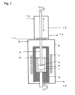
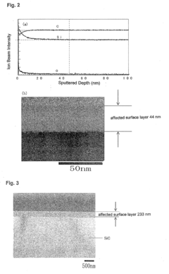
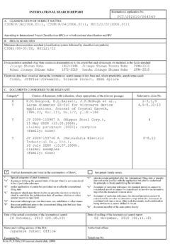
- The method involves controlling the oxygen concentration in the SiC single crystal portion to reduce the thickness of the affected surface layer to at most 50 nm, allowing for precise in situ etching and eliminating the subsurface damaged layer and native oxide film, thereby ensuring a smooth epitaxial growth surface.
Sic epitaxial wafer
PatentPendingEP4545691A1
Innovation
- A SiC epitaxial wafer is developed with a specific density range of basal plane dislocations in the substrate (1/cm² to 3000/cm²) and controlled densities of double Shockley type stacking faults and other stacking faults in the epitaxial layer, allowing for estimation of basal plane dislocation positions and numbers.
Supply Chain Resilience for Automotive SiC Components
The automotive industry's reliance on Silicon Carbide (SiC) components has created significant supply chain vulnerabilities that require strategic management. The COVID-19 pandemic exposed critical weaknesses in the global SiC supply chain, with manufacturing disruptions in key production regions causing severe shortages for automotive electronic systems. These disruptions highlighted the industry's overdependence on a limited number of suppliers, primarily concentrated in Asia, creating bottlenecks that impacted vehicle production worldwide.
To address these vulnerabilities, automotive manufacturers and tier-one suppliers are implementing multi-faceted resilience strategies. Supplier diversification has emerged as a primary approach, with companies establishing relationships with SiC wafer manufacturers across different geographical regions to mitigate regional disruption risks. This strategy includes qualifying alternative suppliers and developing standardized qualification processes to accelerate supplier onboarding during shortages.
Vertical integration represents another significant trend, with major automotive companies investing in or acquiring SiC manufacturing capabilities. Companies like Bosch and Infineon have made substantial investments in in-house SiC production facilities to reduce dependency on external suppliers and gain greater control over their supply chains. These investments typically focus on critical components of the SiC value chain, particularly wafer production and device fabrication.
Strategic inventory management has evolved beyond traditional just-in-time approaches, with companies maintaining larger buffer stocks of critical SiC components. Advanced forecasting models utilizing artificial intelligence are being deployed to predict potential supply disruptions and adjust inventory levels accordingly, balancing cost considerations with supply security requirements.
Regional manufacturing diversification is accelerating, with significant investments in SiC production facilities across North America and Europe to complement existing Asian capacity. The CHIPS Act in the United States and similar initiatives in Europe are providing financial incentives and policy support for domestic semiconductor manufacturing, including SiC wafer production specifically targeted at automotive applications.
Collaborative industry initiatives are also emerging, with automotive OEMs, tier-one suppliers, and semiconductor manufacturers forming consortia to address supply chain vulnerabilities collectively. These collaborations focus on developing industry standards, sharing capacity information, and establishing emergency response protocols for future disruptions. Such initiatives aim to create a more transparent and resilient ecosystem for automotive SiC components.
Environmental Impact and Sustainability of SiC Technology
The adoption of Silicon Carbide (SiC) wafers in automotive electronic systems represents a significant advancement in sustainable technology. SiC-based power electronics demonstrate superior energy efficiency compared to traditional silicon-based components, with conversion efficiency improvements of 5-10%. This translates to reduced energy consumption across the vehicle lifecycle, particularly important for electric vehicles where power management directly impacts range and battery life.
Manufacturing processes for SiC wafers have evolved to become increasingly environmentally conscious. While initial production methods were energy-intensive, recent innovations have reduced energy requirements by approximately 30% compared to early manufacturing techniques. Water usage in SiC wafer fabrication has similarly decreased, with closed-loop systems now recovering up to 80% of process water in advanced facilities.
The durability of SiC components contributes significantly to sustainability through extended product lifecycles. SiC-based power modules in automotive applications typically demonstrate 2-3 times longer operational lifespans than silicon equivalents under high-temperature conditions. This longevity reduces electronic waste generation and decreases the environmental footprint associated with replacement part manufacturing and distribution.
End-of-life considerations for SiC wafers present both challenges and opportunities. The chemical stability of silicon carbide makes traditional recycling methods less effective, necessitating specialized processes. However, the high value of recovered materials justifies investment in advanced recycling technologies. Current recovery rates for precious metals from SiC electronic components reach approximately 85-90% in state-of-the-art facilities.
Carbon footprint analyses of automotive systems utilizing SiC technology show promising results. Life cycle assessments indicate that despite higher initial manufacturing emissions, the operational efficiency gains of SiC-based systems result in net carbon reductions within 1-3 years of vehicle operation. For electric vehicles specifically, SiC power electronics can reduce total lifetime carbon emissions by 5-8% through improved charging and power conversion efficiency.
Supply chain sustainability remains an area requiring continued attention. The geographic concentration of raw materials for SiC production presents potential environmental and social risks. Industry leaders have begun implementing responsible sourcing initiatives, with approximately 60% of major SiC manufacturers now publishing sustainability reports that address material provenance and environmental impact mitigation strategies.
Unlock deeper insights with Patsnap Eureka Quick Research — get a full tech report to explore trends and direct your research. Try now!
Generate Your Research Report Instantly with AI Agent
Supercharge your innovation with Patsnap Eureka AI Agent Platform!