Analysis of Silicon Carbide Wafer Conductivity in Electric Motors
OCT 14, 20259 MIN READ
Generate Your Research Report Instantly with AI Agent
Patsnap Eureka helps you evaluate technical feasibility & market potential.
SiC Wafer Technology Evolution and Objectives
Silicon carbide (SiC) wafer technology has undergone remarkable evolution since its initial development in the early 20th century. The journey began with the Acheson process in 1891, which provided the first commercial method for SiC production. However, it wasn't until the 1950s that researchers began exploring SiC's semiconductor properties for electronic applications. The 1980s marked a significant turning point with the development of the modified Lely method, enabling the production of higher quality SiC crystals.
The 1990s witnessed the emergence of commercial SiC wafer production, though limited to small diameters and containing substantial defects. By the early 2000s, 3-inch SiC wafers became commercially viable, followed by 4-inch wafers in the mid-2000s. The industry achieved another milestone with 6-inch wafer production becoming mainstream around 2015, while 8-inch wafers are currently transitioning from research to commercial production.
The technological evolution has been driven by the superior properties of SiC compared to traditional silicon, particularly for power electronics applications. SiC offers approximately ten times higher breakdown electric field strength, three times wider bandgap, and three times higher thermal conductivity than silicon. These properties make SiC exceptionally suitable for high-temperature, high-power, and high-frequency applications, including electric motor drives.
In electric motor applications, SiC wafer conductivity plays a crucial role in determining the efficiency and performance of power electronic components. The evolution of SiC wafer technology has focused on improving several key parameters: reducing defect density (particularly micropipes and basal plane dislocations), enhancing crystal quality, increasing wafer diameter for economies of scale, and optimizing doping profiles to achieve desired conductivity characteristics.
The primary technological objectives for SiC wafer development in electric motor applications include achieving uniform conductivity across larger wafer diameters, reducing wafer costs through improved manufacturing yields, developing more precise doping techniques for optimal carrier concentration, and minimizing crystal defects that impact electrical performance. Additionally, there is significant focus on improving the interface quality between SiC and its oxide, which remains a challenge for device reliability.
Looking forward, the industry aims to achieve commercial viability of 8-inch and potentially 12-inch SiC wafers, further reduce defect densities below 0.1/cm², develop more sophisticated epitaxial growth techniques for precise conductivity control, and establish more standardized testing methodologies for wafer conductivity characterization. These advancements will be critical in meeting the growing demands of electric vehicle motors and industrial drive systems, where efficiency, power density, and reliability are paramount considerations.
Market Demand for SiC in Electric Motor Applications
The global market for Silicon Carbide (SiC) in electric motor applications has witnessed exponential growth in recent years, primarily driven by the rapid expansion of electric vehicles (EVs) and industrial automation sectors. Current market valuations indicate that the SiC power semiconductor market reached approximately 1.5 billion USD in 2022, with projections suggesting a compound annual growth rate of 18-20% through 2030, potentially reaching 6 billion USD by the end of the decade.
Electric vehicle manufacturers represent the largest demand segment, accounting for nearly 60% of SiC consumption in motor applications. This demand stems from SiC's superior thermal conductivity and higher breakdown field strength compared to traditional silicon, enabling more efficient power conversion and motor control systems. Tesla's adoption of SiC-based inverters in their Model 3 and subsequent models marked a significant inflection point in market demand, with other major automotive manufacturers following suit.
Industrial motor applications constitute the second-largest market segment at approximately 25% of total demand. The push for energy efficiency in manufacturing processes has accelerated the adoption of SiC-based variable frequency drives (VFDs) and motor controllers. Industries with continuous operation requirements, such as oil and gas, mining, and heavy manufacturing, have demonstrated particular interest due to the potential for significant energy savings over equipment lifetimes.
Regional analysis reveals that Asia-Pacific, particularly China, Japan, and South Korea, leads in SiC demand for motor applications, representing approximately 45% of the global market. This dominance is attributed to the region's robust EV manufacturing ecosystem and government policies promoting electrification. North America and Europe follow with approximately 30% and 20% market share respectively, with both regions showing accelerated adoption rates.
Supply chain constraints remain a significant factor influencing market dynamics. The complex manufacturing process for SiC wafers, requiring specialized equipment and expertise, has created bottlenecks that manufacturers are racing to address. Major suppliers like Wolfspeed, STMicroelectronics, and Rohm Semiconductor have announced capacity expansion plans, with combined investments exceeding 5 billion USD over the next five years.
Price sensitivity analysis indicates that while SiC components currently command a premium of 2-3 times over silicon alternatives, this gap is expected to narrow as manufacturing scales and yields improve. Market research suggests that price parity with silicon for certain applications could be achieved by 2028, potentially triggering even more widespread adoption across additional motor applications including HVAC systems, home appliances, and smaller industrial motors.
Current Challenges in SiC Wafer Conductivity
Silicon carbide (SiC) wafer conductivity presents several significant challenges that impede its optimal implementation in electric motor applications. The primary obstacle remains the high defect density in commercially available SiC wafers. These defects, including micropipes, dislocations, and stacking faults, directly impact electrical conductivity properties and compromise overall performance reliability. Current manufacturing processes struggle to consistently produce wafers with defect densities below 1 per cm², whereas ideal applications in high-performance electric motors require densities approaching 0.1 per cm² or lower.
Thermal management during operation represents another critical challenge. SiC wafers exhibit excellent thermal conductivity theoretically, but practical implementations reveal conductivity variations across the wafer surface that can lead to hotspot formation. These thermal gradients induce mechanical stress and potentially accelerate device degradation, particularly problematic in the high-current environments typical of electric motor applications.
Interface resistance between SiC wafers and metal contacts presents persistent difficulties. The formation of reliable, low-resistance ohmic contacts remains technically challenging due to the wide bandgap nature of SiC. Current metallization techniques often result in contact resistances that are 2-3 times higher than theoretical minimums, creating power losses that diminish the efficiency advantages SiC should provide in electric motor systems.
Wafer uniformity across large diameters (150mm and above) continues to challenge manufacturers. Conductivity variations of up to 15% have been observed across single wafers, making it difficult to achieve consistent performance in large-area devices necessary for high-power electric motor applications. This non-uniformity complicates device design and reduces manufacturing yield.
Cost factors remain prohibitive for widespread adoption. Current SiC wafer production costs exceed those of silicon wafers by approximately 8-10 times, primarily due to complex manufacturing processes and lower yields. While performance benefits justify this premium in some high-end applications, the cost barrier significantly limits broader implementation in mainstream electric motor markets.
Doping control precision presents technical hurdles that directly affect conductivity properties. Achieving precise carrier concentrations throughout the wafer volume requires sophisticated implantation and annealing processes that are not yet fully optimized. Variations in doping concentration can lead to unpredictable conductivity behavior under the high-voltage, high-temperature conditions typical in electric motor operations.
Finally, long-term reliability under cyclic loading conditions remains inadequately characterized. SiC wafers in electric motor applications experience repeated thermal and electrical stress cycles that can gradually alter conductivity properties. Current accelerated testing methodologies have not fully captured these long-term effects, creating uncertainty about device lifetime predictions in real-world applications.
Current Methods for Enhancing SiC Wafer Conductivity
01 Doping techniques for controlling SiC wafer conductivity
Various doping methods are employed to control the electrical conductivity of silicon carbide wafers. These techniques include ion implantation, epitaxial growth with controlled dopant incorporation, and thermal diffusion processes. By precisely controlling the type and concentration of dopants such as nitrogen, phosphorus, aluminum, or boron, manufacturers can achieve specific conductivity levels ranging from semi-insulating to highly conductive properties, which are crucial for different electronic device applications.- Doping techniques for controlling SiC wafer conductivity: Various doping methods are employed to control the conductivity of silicon carbide wafers. These techniques include ion implantation, epitaxial growth with controlled dopant concentration, and in-situ doping during crystal growth. By precisely controlling the type and concentration of dopants such as nitrogen, phosphorus, aluminum, or boron, manufacturers can achieve specific conductivity levels ranging from semi-insulating to highly conductive properties, which are essential for different electronic applications.
- Crystal growth methods affecting conductivity properties: The crystal growth method significantly impacts the conductivity characteristics of silicon carbide wafers. Physical vapor transport (PVT), chemical vapor deposition (CVD), and modified Lely methods each produce crystals with different defect densities and impurity concentrations. These factors directly influence carrier mobility and electrical conductivity. Advanced growth techniques focus on reducing micropipe defects and controlling polytype formation to achieve more uniform conductivity across the wafer surface.
- Surface treatment methods to enhance conductivity: Various surface treatments are applied to silicon carbide wafers to modify their conductivity characteristics. These include high-temperature annealing, chemical-mechanical polishing (CMP), and plasma treatments. Such processes can reduce surface defects, remove damaged layers, and activate dopants, thereby enhancing carrier mobility and improving overall conductivity. Surface passivation techniques are also employed to stabilize the electrical properties and prevent degradation over time.
- Polytype engineering for conductivity control: Silicon carbide exists in multiple polytypes (4H, 6H, 3C, etc.) with inherently different electrical properties. Controlling the formation of specific polytypes during crystal growth allows for tailored conductivity characteristics. The 4H polytype generally offers higher electron mobility compared to 6H, while 3C-SiC provides different conductivity profiles. Advanced techniques focus on stabilizing desired polytypes and minimizing unwanted polytype inclusions to achieve consistent electrical performance across wafers.
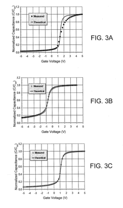
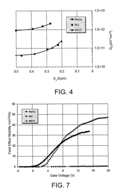
- Measurement and characterization of SiC wafer conductivity: Specialized techniques for measuring and characterizing silicon carbide wafer conductivity include four-point probe testing, Hall effect measurements, capacitance-voltage profiling, and contactless resistivity mapping. These methods enable precise evaluation of conductivity distribution across wafers, identification of defects affecting electrical properties, and verification of doping profiles. Advanced imaging techniques such as deep-level transient spectroscopy help identify traps and recombination centers that impact carrier mobility and overall conductivity performance.
02 Crystal growth methods affecting conductivity properties
The crystal growth process significantly impacts the conductivity characteristics of silicon carbide wafers. Methods such as physical vapor transport (PVT), modified Lely method, and chemical vapor deposition (CVD) create different defect structures and impurity distributions that influence electrical properties. Advanced growth techniques focus on reducing micropipes, dislocations, and stacking faults that can disrupt carrier transport and degrade conductivity uniformity across the wafer surface.Expand Specific Solutions03 Surface treatment methods for enhancing conductivity
Various surface treatment processes are employed to optimize the conductivity of silicon carbide wafers. These include chemical-mechanical polishing (CMP), high-temperature annealing, hydrogen etching, and surface passivation techniques. Such treatments remove damaged layers, reduce surface states, and create atomically smooth surfaces that minimize carrier scattering and contact resistance, thereby enhancing the overall electrical performance of devices fabricated on these wafers.Expand Specific Solutions04 Polytypes and crystallographic orientation effects on conductivity
Different silicon carbide polytypes (4H-SiC, 6H-SiC, 3C-SiC) exhibit varying electrical conductivity properties due to their unique band structures and carrier mobilities. The crystallographic orientation of the wafer also significantly affects conductivity characteristics, with certain planes showing preferential carrier transport. These polytype-specific properties allow for tailored conductivity profiles suited for specific applications such as high-power electronics, high-frequency devices, or high-temperature sensors.Expand Specific Solutions05 Measurement and characterization techniques for conductivity
Advanced measurement methods are essential for accurately characterizing silicon carbide wafer conductivity. These include four-point probe testing, Hall effect measurements, capacitance-voltage profiling, and contactless resistivity mapping. Non-destructive evaluation techniques allow for comprehensive conductivity mapping across entire wafers, enabling manufacturers to identify spatial variations, verify doping uniformity, and ensure consistent electrical performance for device fabrication.Expand Specific Solutions
Leading Manufacturers and Research Institutions
The Silicon Carbide (SiC) wafer market for electric motors is currently in a growth phase, with increasing adoption driven by superior conductivity properties that enhance motor efficiency. The global market is expanding rapidly, projected to reach significant scale as electric vehicle adoption accelerates. Technologically, the field shows moderate maturity with established players like Wolfspeed, Infineon, and STMicroelectronics leading commercial production, while companies such as RESONAC, TanKeBlue, and GeneSiC are advancing manufacturing capabilities. Regional competition is intensifying with Japanese firms (Toshiba, Mitsubishi Electric) and Chinese enterprises (Zhuzhou CRRC Times Semiconductor) investing heavily. The competitive landscape features both specialized SiC producers and diversified semiconductor manufacturers seeking to capitalize on the transition to wide-bandgap semiconductor technologies for next-generation electric powertrains.
Wolfspeed, Inc.
Technical Solution: Wolfspeed has pioneered 150mm silicon carbide wafer technology with industry-leading low defect density and high conductivity profiles specifically optimized for electric motor applications. Their proprietary high-purity manufacturing process achieves carrier mobility exceeding 900 cm²/V·s and resistivity uniformity variation below 10% across wafers[1]. The company's vertical integration strategy encompasses substrate growth, epitaxy, and device fabrication, enabling tight control over electrical properties. Their latest generation SiC MOSFETs feature on-resistance as low as 1.7mΩ·cm² and switching speeds up to 100kHz while maintaining thermal stability at junction temperatures of 200°C[2], making them ideal for high-efficiency motor drive inverters that can achieve 99% efficiency.
Strengths: Industry-leading SiC substrate quality with lowest micropipe density (<1/cm²); comprehensive vertical integration from material to device; established manufacturing scale with proven reliability data. Weaknesses: Higher cost structure compared to silicon alternatives; limited geographic manufacturing diversification creating supply chain vulnerabilities; longer lead times during industry-wide capacity constraints.
STMicroelectronics International NV
Technical Solution: STMicroelectronics has developed advanced silicon carbide technology specifically tailored for electric motor applications through their STPOWER SiC platform. Their manufacturing process incorporates proprietary defect engineering techniques that reduce stacking faults by over 80% compared to conventional methods, resulting in enhanced carrier mobility and more uniform conductivity profiles[5]. ST's SiC wafers feature optimized doping concentration gradients that maintain consistent electrical characteristics even under the high-temperature cycling conditions typical in electric motors. Their third-generation SiC MOSFETs achieve specific on-resistance values below 2.5mΩ·cm² with gate oxide reliability exceeding 20 years at maximum rated conditions[6]. ST has also pioneered advanced SiC module packaging with sintered silver die-attach technology that reduces thermal resistance by 30% compared to conventional soldering, enabling higher current densities in motor drive applications.
Strengths: Vertically integrated manufacturing from substrate to packaged devices; extensive automotive qualification experience; advanced multi-level module designs optimized for motor drives. Weaknesses: More limited wafer diameter offerings compared to some competitors; higher variability in electrical parameters across production lots; relatively higher thermal resistance in some package configurations.
Key Patents and Breakthroughs in SiC Conductivity
Methods of forming sic mosfets with high inversion layer mobility
PatentActiveUS20100221924A1
Innovation
- Thermally growing an oxide layer on silicon carbide and annealing it in a nitric oxide environment at temperatures greater than 1175°C, with controlled oxidation rates and metallic impurities present, to reduce interface trap density and enhance channel mobility.
Reducing nitrogen content in silicon carbide crystals by sublimation growth in a hydrogen-containing ambient
PatentInactiveEP1664395B1
Innovation
- A sublimation growth method using a hydrogen-containing ambient atmosphere in the growth chamber, where hydrogen gas is introduced at specific pressures and flow rates to control the nitrogen content by reducing carbon-vacancy sites and passivating the silicon carbide growth surface, thereby minimizing nitrogen incorporation.
Thermal Management Solutions for SiC-Based Motors
Thermal management represents a critical challenge in the development and operation of Silicon Carbide (SiC)-based electric motors. The superior thermal conductivity of SiC wafers, approximately three times that of silicon, creates both opportunities and challenges for motor design engineers. Effective thermal solutions must address the unique characteristics of SiC power electronics while maximizing their performance benefits.
Current thermal management approaches for SiC-based motors include advanced cooling systems that utilize direct liquid cooling technologies. These systems circulate coolants directly across SiC power modules, achieving thermal resistance values as low as 0.15°C/W. This represents a significant improvement over traditional air-cooled systems that typically exhibit thermal resistance values of 0.4-0.6°C/W.
Double-sided cooling architectures have emerged as particularly effective for SiC applications. By removing heat from both sides of the SiC wafer simultaneously, these designs can handle the higher power densities enabled by SiC technology. Implementation typically involves specialized packaging techniques that maintain electrical isolation while maximizing thermal transfer paths.
Phase-change materials (PCMs) integrated into motor housings provide thermal buffering during transient high-power operations. These materials absorb excess heat during peak loads and release it gradually during lower-demand periods. For SiC-based motors operating in variable load conditions, PCMs with melting points between 80-120°C have demonstrated optimal performance characteristics.
Advanced thermal interface materials (TIMs) with enhanced thermal conductivity values of 5-10 W/m·K are increasingly utilized between SiC modules and cooling structures. Nano-enhanced composites incorporating boron nitride or aluminum oxide particles have shown particular promise in maintaining performance under the thermal cycling conditions typical of electric motor operation.
Computational fluid dynamics (CFD) modeling has become essential for optimizing thermal management solutions for SiC-based motors. These simulations enable designers to predict hotspot formation and optimize coolant flow patterns before physical prototyping. Recent models incorporating junction temperature mapping capabilities can predict temperature distributions with accuracy within ±3°C under dynamic operating conditions.
Integrated thermal sensors and adaptive cooling control systems represent the cutting edge of SiC motor thermal management. These systems continuously monitor junction temperatures and adjust cooling parameters in real-time, preventing thermal runaway while maximizing performance. Implementation typically involves embedding temperature sensors directly within SiC modules and developing sophisticated control algorithms that balance cooling needs with energy efficiency.
Environmental Impact and Sustainability Considerations
The adoption of Silicon Carbide (SiC) wafers in electric motor applications presents significant environmental and sustainability advantages compared to traditional silicon-based semiconductors. SiC technology enables more efficient power conversion, resulting in reduced energy losses during motor operation. This efficiency improvement translates directly to lower energy consumption across the lifecycle of electric vehicles and industrial systems, contributing to reduced carbon emissions and resource utilization.
Manufacturing processes for SiC wafers currently require substantial energy inputs, with temperatures exceeding 2000°C needed for crystal growth. This energy-intensive production creates a notable carbon footprint that partially offsets the operational benefits. However, ongoing advancements in manufacturing techniques, including optimized furnace designs and more efficient crystal growth methods, are progressively reducing the environmental impact of production.
The extended temperature tolerance and higher breakdown voltage of SiC wafers contribute significantly to sustainability through improved product longevity. Electric motors utilizing SiC components demonstrate enhanced durability under thermal stress conditions, extending operational lifespans by an estimated 20-30% compared to conventional silicon alternatives. This longevity reduces replacement frequency and associated manufacturing demands, decreasing overall resource consumption and electronic waste generation.
Resource efficiency represents another critical environmental consideration. SiC wafers enable the design of smaller, lighter electric motors that maintain equivalent power outputs. This miniaturization reduces material requirements across the supply chain, from raw material extraction to manufacturing and transportation. Additionally, SiC-based systems typically require fewer peripheral components for thermal management, further reducing material consumption and simplifying end-of-life recycling processes.
End-of-life management presents both challenges and opportunities. While SiC materials are chemically stable and non-toxic, specialized recycling infrastructure for recovering valuable materials from SiC wafers remains underdeveloped. Current recycling rates for semiconductor components in electric motors remain below 20%, highlighting a significant opportunity for improvement. Developing effective recovery methods for SiC materials could establish closed-loop material cycles that further enhance the technology's sustainability profile.
Regulatory frameworks increasingly emphasize lifecycle environmental performance, with policies like the European Union's Ecodesign Directive and various carbon pricing mechanisms influencing market adoption. SiC wafer technology aligns well with these regulatory trends, potentially accelerating market penetration as environmental compliance becomes a more significant competitive factor in electric motor applications.
Unlock deeper insights with Patsnap Eureka Quick Research — get a full tech report to explore trends and direct your research. Try now!
Generate Your Research Report Instantly with AI Agent
Supercharge your innovation with Patsnap Eureka AI Agent Platform!