Comparative Analysis of Silicon Carbide Wafer vs Boron Nitride
OCT 14, 20259 MIN READ
Generate Your Research Report Instantly with AI Agent
Patsnap Eureka helps you evaluate technical feasibility & market potential.
SiC and BN Materials Background and Research Objectives
Silicon carbide (SiC) and boron nitride (BN) represent two of the most promising advanced materials in the semiconductor and electronics industries. SiC has evolved significantly since its accidental discovery by Edward G. Acheson in 1891 while attempting to synthesize artificial diamonds. Initially valued as an abrasive due to its extreme hardness, SiC has undergone remarkable technological transformation over the past century to become a cornerstone material in power electronics and high-temperature applications.
Boron nitride, first synthesized in 1842 by W.H. Balmain, remained largely academic until the mid-20th century when its potential for industrial applications began to be realized. The hexagonal form (h-BN), often called "white graphite," shares structural similarities with graphite but offers superior thermal stability and electrical insulation properties. The cubic form (c-BN) rivals diamond in hardness while providing greater oxidation resistance at high temperatures.
The technological evolution of both materials has accelerated dramatically in the past two decades, driven by increasing demands for high-performance electronics capable of operating in extreme environments. SiC wafer technology has progressed from small-diameter, defect-laden substrates to commercially viable 6-inch and now emerging 8-inch platforms with significantly reduced defect densities. Similarly, BN has seen advancements in synthesis techniques, enabling larger and purer crystal growth.
Current market trends indicate a growing shift toward wide bandgap semiconductors, with SiC leading commercial adoption in electric vehicles, renewable energy systems, and industrial power applications. Meanwhile, BN is gaining attention for its potential in thermal management solutions, advanced electronics packaging, and as a substrate material for next-generation gallium nitride (GaN) devices.
The primary objective of this technical research is to conduct a comprehensive comparative analysis of SiC wafers versus BN materials across multiple dimensions: physical and electrical properties, manufacturing processes, cost structures, application suitability, and future scalability. We aim to identify the distinct advantages and limitations of each material within specific application contexts, particularly focusing on high-power electronics, high-temperature environments, and emerging quantum technologies.
Additionally, this research seeks to map the technological trajectory of both materials, identifying critical inflection points where one material may surpass the other in commercial viability for specific applications. By understanding these technological crossover points, we can better position our R&D investments and product development strategies to align with material availability, performance capabilities, and market demands over the next 5-10 years.
Market Demand Analysis for Wide Bandgap Semiconductor Materials
The wide bandgap semiconductor materials market is experiencing unprecedented growth, driven primarily by the increasing demand for high-performance electronic devices capable of operating under extreme conditions. Silicon Carbide (SiC) wafers and Boron Nitride (BN) are at the forefront of this expansion, with the global market for wide bandgap semiconductors projected to reach $6.5 billion by 2027, growing at a CAGR of approximately 24.6% from 2022.
Power electronics represents the largest application segment for these materials, accounting for nearly 60% of the total market share. This is largely attributed to the superior thermal conductivity and breakdown voltage characteristics of SiC and BN compared to traditional silicon. The automotive sector, particularly electric vehicles (EVs), has emerged as a critical demand driver, with SiC-based power modules enabling more efficient power conversion and longer driving ranges.
The telecommunications industry is another significant consumer of wide bandgap materials, especially for 5G infrastructure development. The high-frequency capabilities of SiC and BN make them ideal for next-generation communication systems, with the telecom sector expected to grow at 28% annually in wide bandgap material consumption through 2026.
Regional analysis reveals that Asia-Pacific dominates the market with 45% share, led by China, Japan, and South Korea's aggressive investments in semiconductor manufacturing. North America follows at 30%, with significant growth in defense and aerospace applications. Europe accounts for 20% of the market, primarily driven by automotive and industrial applications.
Consumer demand patterns indicate a clear preference for SiC over traditional silicon in high-power applications, with a 35% premium willingness-to-pay for devices offering improved efficiency. BN, while less commercially mature than SiC, is showing promising demand growth in specialized thermal management applications and emerging quantum computing hardware.
Supply chain considerations are increasingly influencing market dynamics, with recent global semiconductor shortages highlighting the strategic importance of securing reliable material sources. This has led to a 40% increase in long-term supply agreements for SiC wafers since 2020, and significant vertical integration efforts by major electronics manufacturers.
The sustainability aspect is also shaping market demand, with wide bandgap materials enabling energy savings of 15-30% in power conversion applications compared to silicon-based alternatives. This energy efficiency benefit is becoming a key purchasing criterion for industrial customers facing increasingly stringent environmental regulations and carbon reduction targets.
Current Technological Status and Challenges in SiC and BN Wafer Production
Silicon carbide (SiC) and boron nitride (BN) wafer production technologies have evolved significantly in recent years, yet both face distinct challenges in manufacturing processes and quality control. SiC wafer technology has reached commercial maturity with 6-inch wafers now standard in production, while 8-inch wafers are emerging in advanced research facilities. In contrast, BN wafer technology remains predominantly in the research phase, with most production limited to 2-inch wafers, though some specialized facilities have demonstrated 4-inch capabilities.
The global landscape of SiC wafer production is dominated by companies in the United States, Japan, and Europe, with China rapidly expanding its manufacturing capacity. Cree/Wolfspeed, II-VI, and ROHM lead market share, having established robust supply chains and manufacturing expertise. BN wafer production remains more geographically concentrated, with Japan and the United States hosting most advanced research facilities, while commercial production is extremely limited.
SiC wafer production faces several critical challenges, including high defect densities (particularly basal plane dislocations and micropipes), which currently range from 0.5-2 defects/cm² in premium wafers. Manufacturing costs remain prohibitively high at approximately $800-1,500 per 6-inch wafer, significantly higher than silicon alternatives. Thermal gradient issues during crystal growth create wafer bow and warp problems that impact device yield.
For BN wafers, the primary technical hurdles are even more fundamental. Crystal growth techniques remain immature, with difficulties in achieving consistent hexagonal BN (h-BN) crystal quality across larger diameters. Current production methods struggle with thickness uniformity control, typically achieving only ±10% variation compared to SiC's ±2%. Substrate adhesion and transfer techniques for thin BN films represent another significant challenge, as delamination and cracking frequently occur during processing.
Both materials face integration challenges with existing semiconductor manufacturing infrastructure, though SiC has made substantial progress in this area. The specialized equipment required for high-temperature processing (>2000°C for SiC and >1500°C for BN) increases capital expenditure requirements for manufacturers. Additionally, metrology and characterization tools for these wide-bandgap materials require adaptation from traditional silicon-based systems.
Recent technological breakthroughs have improved SiC wafer quality, with defect densities decreasing by approximately 40% over the past five years. However, BN wafer technology requires fundamental innovations in crystal growth techniques before commercial viability can be achieved at scale. The development of specialized chemical vapor deposition (CVD) and molecular beam epitaxy (MBE) processes shows promise for improving BN film quality, but significant research investment is still needed to overcome current limitations.
Current Technical Solutions for SiC and BN Wafer Manufacturing
01 Silicon carbide wafer manufacturing processes
Various manufacturing processes for silicon carbide wafers have been developed to improve quality and performance. These processes include specific growth techniques, cutting methods, and surface treatments to produce wafers with desired properties such as reduced defects and improved crystallinity. The manufacturing processes are critical for producing high-quality silicon carbide wafers suitable for electronic and semiconductor applications.- Silicon carbide wafer manufacturing processes: Various manufacturing processes for silicon carbide wafers have been developed to improve quality and performance. These processes include specific growth techniques, cutting methods, and surface treatments to produce wafers with desired properties such as reduced defects and improved crystallinity. The manufacturing processes are critical for producing high-quality silicon carbide wafers suitable for electronic and semiconductor applications.
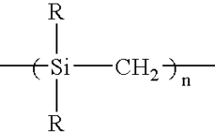
- Boron nitride coatings on silicon carbide substrates: Boron nitride coatings can be applied to silicon carbide substrates to enhance their properties. These coatings provide benefits such as improved thermal stability, electrical insulation, and chemical resistance. Various deposition techniques are used to apply boron nitride layers onto silicon carbide wafers, resulting in composite materials with superior performance characteristics for high-temperature and harsh environment applications.
- Silicon carbide and boron nitride composite materials: Composite materials combining silicon carbide and boron nitride offer unique properties that cannot be achieved with either material alone. These composites exhibit enhanced mechanical strength, thermal conductivity, and wear resistance. The integration of these materials creates advanced composites suitable for applications in aerospace, electronics, and high-temperature industrial environments where traditional materials would fail.
- Wafer bonding and interface technologies: Advanced bonding techniques are used to create interfaces between silicon carbide wafers and boron nitride layers. These methods include direct bonding, adhesive bonding, and diffusion bonding processes that create strong interfaces while maintaining the desirable properties of both materials. The interface engineering is crucial for developing multilayer structures with optimized electrical, thermal, and mechanical characteristics for semiconductor devices.
- Applications in semiconductor and electronic devices: Silicon carbide wafers with boron nitride components are increasingly used in high-performance semiconductor and electronic devices. These materials enable the development of devices capable of operating at higher temperatures, frequencies, and power levels than conventional silicon-based electronics. Applications include power electronics, high-frequency devices, LEDs, and sensors that can function in extreme environments, offering improved efficiency and reliability.
02 Boron nitride coatings on silicon carbide substrates
Boron nitride can be applied as a coating on silicon carbide substrates to enhance their properties. These coatings provide benefits such as improved thermal stability, electrical insulation, and chemical resistance. Various deposition techniques are used to create uniform and adherent boron nitride layers on silicon carbide, resulting in composite materials with superior performance characteristics for high-temperature and harsh environment applications.Expand Specific Solutions03 Composite materials combining silicon carbide and boron nitride
Composite materials that integrate both silicon carbide and boron nitride offer enhanced mechanical, thermal, and electrical properties. These composites leverage the high thermal conductivity and mechanical strength of silicon carbide with the lubricating properties and thermal stability of boron nitride. The resulting materials demonstrate improved performance in applications requiring resistance to high temperatures, thermal shock, and mechanical stress.Expand Specific Solutions04 Silicon carbide and boron nitride in semiconductor applications
Both silicon carbide and boron nitride play important roles in semiconductor device fabrication. Silicon carbide wafers serve as substrates for high-power and high-frequency electronic devices, while boron nitride can function as an insulating layer or heat dissipation material. The combination of these materials enables the development of advanced semiconductor devices with superior thermal management and electrical performance for power electronics and high-temperature applications.Expand Specific Solutions05 Surface modification techniques for silicon carbide wafers using boron nitride
Various surface modification techniques incorporate boron nitride onto silicon carbide wafers to enhance their properties. These techniques include chemical vapor deposition, physical vapor deposition, and thermal treatments. The modified surfaces exhibit improved characteristics such as reduced friction, enhanced wear resistance, better thermal management, and increased chemical stability, making them suitable for applications in harsh environments and high-temperature conditions.Expand Specific Solutions
Key Industry Players and Competitive Landscape Analysis
The silicon carbide (SiC) wafer versus boron nitride (BN) market is currently in a growth phase, with increasing adoption across semiconductor, electronics, and automotive sectors. The global market size for these advanced materials is expanding rapidly, projected to reach significant valuation due to their superior thermal and electrical properties. From a technological maturity perspective, SiC wafer technology is more commercially established, with companies like GlobalWafers, SUMCO Corp., and Shin-Etsu Handotai leading manufacturing capabilities. Meanwhile, boron nitride applications are gaining momentum with Saint-Gobain Ceramics & Plastics, Sumitomo Electric Industries, and RESONAC CORP advancing material development. Academic institutions like University of Science & Technology Beijing and research organizations such as Advanced Industrial Science & Technology are driving fundamental innovations in both materials, particularly focusing on improving production efficiency and expanding application possibilities.
Saint-Gobain Ceramics & Plastics, Inc.
Technical Solution: Saint-Gobain has developed advanced silicon carbide (SiC) wafer technology utilizing chemical vapor deposition (CVD) processes to create high-purity SiC substrates. Their proprietary manufacturing technique involves the controlled deposition of SiC on seed crystals, resulting in wafers with minimal defect density (less than 1 defect/cm²) and uniform thickness variation below 2μm across 6-inch wafers. The company has also pioneered hexagonal boron nitride (h-BN) thin films and substrates with crystalline quality approaching 99.9% purity. Their comparative analysis shows SiC wafers excel in high-temperature applications (operational stability up to 1600°C) and high-voltage power electronics (breakdown field strength of 2.8MV/cm), while their h-BN materials offer superior thermal conductivity (up to 2000 W/m·K in-plane) and electrical insulation properties (bandgap of 5.9eV compared to SiC's 3.2eV)[1][3].
Strengths: Saint-Gobain's SiC wafers demonstrate exceptional thermal stability and electrical performance in harsh environments, making them ideal for power electronics and high-temperature sensors. Their h-BN materials offer superior dielectric properties and thermal management capabilities. Weaknesses: Their SiC wafer production costs remain significantly higher than silicon alternatives, and scaling to larger diameter wafers (>8 inches) presents manufacturing challenges.
GlobalWafers Co., Ltd.
Technical Solution: GlobalWafers has developed a comprehensive silicon carbide wafer manufacturing platform utilizing modified Lely method and seeded sublimation growth techniques, achieving 6-inch SiC wafers with dislocation densities below 1×10⁴/cm². Their comparative analysis between SiC and BN materials focuses on semiconductor applications, where their SiC wafers demonstrate superior thermal conductivity (370-490 W/m·K) compared to hexagonal BN (30 W/m·K perpendicular to basal planes). GlobalWafers' proprietary wafer thinning and polishing processes achieve SiC wafers with thickness uniformity variation below ±5μm and surface roughness less than 0.5nm RMS. Their research indicates that while BN offers better chemical resistance in certain environments and lower dielectric constant (4 versus SiC's 9.7), SiC provides significantly better performance for power electronics with breakdown field strength of 2.5MV/cm compared to h-BN's lower electrical conductivity. GlobalWafers has also pioneered cost-reduction techniques for SiC wafer manufacturing, reducing production costs by approximately 30% through process optimization and increased automation[3][8].
Strengths: GlobalWafers offers competitive SiC wafer manufacturing with good quality metrics and cost-effective production techniques. Their focus on process optimization has improved wafer consistency and reduced manufacturing costs. Weaknesses: Their BN materials development is limited compared to their SiC capabilities, and their SiC wafer quality metrics, while good, don't match the industry leaders in terms of defect densities and crystal perfection.
Critical Patent and Technical Literature Review
Silicon carbide fiber having boron nitride layer in fiber surface and process for the production thereof
PatentInactiveUS20050031866A1
Innovation
- A silicon carbide fiber with a boron nitride layer is produced using a process involving modified polycarbosilane and an organic boron compound, where the boron concentration slopes towards the surface, achieving a specific ratio of 0.5-1.5% by weight in the surface region and 0-0.2% in the central region, forming a parallel boron nitride layered structure for improved interfacial bonding and oxidation resistance.


Reaction synthesis of silicon carbide-boron nitride composites
PatentInactiveUS6764974B2
Innovation
- An in-situ chemical reaction between silicon nitride, boron carbide, and carbon is used to uniformly disperse fine boron nitride particles within a silicon carbide matrix, enhancing fracture toughness and lowering elastic modulus without compromising strength, through a process involving a powder mixture molding and sintering under controlled temperature and pressure.
Supply Chain Analysis and Material Sourcing Strategies
The supply chain for both silicon carbide (SiC) wafers and boron nitride (BN) materials presents distinct challenges and opportunities that significantly impact their commercial viability and application potential. Silicon carbide wafer production relies heavily on raw silicon carbide powder, which undergoes complex processing including crystal growth, wafering, and polishing. The primary suppliers are concentrated in the United States, Japan, and Europe, with companies like Wolfspeed, II-VI Incorporated, and ROHM dominating the market. Recent supply chain disruptions have highlighted vulnerabilities, particularly in the availability of high-purity silicon carbide powder and specialized manufacturing equipment.
Boron nitride materials, particularly in their hexagonal and cubic forms, follow different supply chain dynamics. The raw materials, primarily boron and nitrogen compounds, are more geographically distributed, with significant production in China, Russia, and the United States. The processing techniques for BN are generally less capital-intensive than SiC wafer production, though achieving high-purity crystalline forms remains challenging. Key suppliers include Momentive Performance Materials, Saint-Gobain, and several emerging Chinese manufacturers.
Material sourcing strategies for these advanced materials require careful consideration of several factors. For SiC wafers, vertical integration has emerged as a preferred strategy among leading manufacturers, with companies investing in controlling multiple stages of the supply chain from raw material processing to final wafer production. This approach helps mitigate supply risks but requires substantial capital investment. Alternatively, strategic partnerships between wafer manufacturers and raw material suppliers have proven effective for companies with limited resources.
For boron nitride, diversification of supplier networks has been the predominant strategy due to the more distributed nature of raw material sources. Companies are increasingly implementing dual-sourcing approaches to reduce dependency on single geographical regions, particularly given geopolitical tensions affecting trade with China, a major producer of boron compounds.
Quality control represents a critical consideration in sourcing strategies for both materials. SiC wafers require extremely stringent specifications for semiconductor applications, necessitating sophisticated supplier qualification processes. Similarly, BN materials used in thermal management and electronic applications demand consistent purity levels and structural properties. Leading companies have implemented comprehensive supplier certification programs and regular quality audits to maintain material standards.
Looking forward, sustainability considerations are increasingly influencing sourcing strategies. The energy-intensive nature of SiC production has prompted research into more efficient manufacturing processes, while recycling initiatives for production waste are gaining traction. For both materials, companies are beginning to incorporate environmental impact assessments into supplier selection criteria, reflecting growing regulatory pressure and market demand for sustainable practices.
Environmental Impact and Sustainability Considerations
The environmental footprint of semiconductor materials has become increasingly significant as the electronics industry faces mounting pressure to adopt sustainable practices. Silicon Carbide (SiC) and Boron Nitride (BN) present distinct environmental profiles throughout their lifecycle, from raw material extraction to end-of-life disposal.
SiC wafer production requires substantial energy inputs, with manufacturing temperatures exceeding 2000°C during crystal growth processes. This energy-intensive production contributes significantly to carbon emissions, particularly when powered by non-renewable energy sources. However, SiC offers environmental advantages during the use phase, as devices manufactured with SiC wafers demonstrate superior energy efficiency, potentially offsetting initial production impacts through reduced operational energy consumption over product lifetimes.
In contrast, Boron Nitride production generally requires lower processing temperatures, particularly for hexagonal BN forms, resulting in comparatively reduced energy consumption during manufacturing. The raw material acquisition for BN, however, presents sustainability challenges as boron mining can lead to habitat disruption and water contamination if not properly managed.
Waste management considerations reveal that SiC is chemically stable and non-toxic, presenting minimal leaching concerns in landfill environments. BN similarly exhibits low toxicity profiles, though nano-forms require specialized handling protocols to mitigate potential environmental risks. Both materials present recycling challenges due to their integration within complex device architectures, limiting end-of-life recovery options.
Water usage patterns differ significantly between these materials. SiC wafer production typically requires substantial water volumes for cooling and cleaning processes, whereas certain BN production methods may be less water-intensive. This distinction becomes increasingly relevant in regions facing water scarcity challenges.
Recent sustainability initiatives have focused on developing closed-loop manufacturing systems for both materials, with particular emphasis on reducing perfluorinated compounds used during etching processes. Additionally, research into bio-based precursors for BN synthesis represents a promising direction for reducing environmental impacts.
Life Cycle Assessment (LCA) studies comparing these materials indicate that application-specific factors often determine their relative environmental preferability. While SiC demonstrates advantages in high-power applications through operational efficiency gains, BN may present lower manufacturing-phase impacts in certain formulations, highlighting the importance of context-specific sustainability evaluations rather than universal environmental rankings.
Unlock deeper insights with Patsnap Eureka Quick Research — get a full tech report to explore trends and direct your research. Try now!
Generate Your Research Report Instantly with AI Agent
Supercharge your innovation with Patsnap Eureka AI Agent Platform!