How Silicon Carbide Wafer Enhances Hydroelectric Power Generation
OCT 14, 20259 MIN READ
Generate Your Research Report Instantly with AI Agent
Patsnap Eureka helps you evaluate technical feasibility & market potential.
SiC Wafer Technology Background and Objectives
Silicon Carbide (SiC) wafer technology represents a significant advancement in semiconductor materials, with a development history spanning over a century since its first synthesis in 1891 by Edward Acheson. The evolution of SiC wafers has accelerated dramatically in the past three decades, transitioning from laboratory curiosities to commercially viable products that are revolutionizing power electronics across multiple industries.
The fundamental properties that make SiC wafers particularly valuable include their wide bandgap (3.2 eV compared to silicon's 1.1 eV), high thermal conductivity (approximately 3-4 times that of silicon), and exceptional breakdown electric field strength (nearly 10 times higher than conventional silicon). These characteristics enable the creation of semiconductor devices capable of operating at higher temperatures, voltages, and frequencies while maintaining smaller form factors and greater efficiency.
In the context of hydroelectric power generation, SiC wafer technology aims to address several critical limitations in conventional systems. Traditional silicon-based power electronics in hydroelectric facilities face efficiency constraints, thermal management challenges, and reliability issues under high-voltage, high-current conditions. The integration of SiC-based devices seeks to overcome these barriers by enabling more efficient power conversion, reducing switching losses, and enhancing overall system reliability.
The technical objectives for SiC wafer implementation in hydroelectric applications include increasing power conversion efficiency by at least 20%, reducing cooling requirements by 30-40%, extending maintenance intervals by 2-3 times current standards, and enabling more compact power electronic systems that can be deployed in space-constrained environments within hydroelectric facilities.
Current technological trajectories indicate a continued refinement in SiC wafer manufacturing processes, with particular focus on increasing wafer diameter (from current 6-inch standards toward 8-inch and beyond), reducing defect densities, and lowering production costs. These advancements are critical to broader adoption in hydroelectric applications, where cost-effectiveness remains a significant consideration alongside performance improvements.
The convergence of SiC wafer technology with hydroelectric power generation represents a strategic intersection of advanced materials science and renewable energy infrastructure. As global energy demands increase alongside requirements for greater efficiency and reduced environmental impact, SiC-based solutions offer a promising pathway to enhance the performance, reliability, and sustainability of hydroelectric power systems through next-generation power electronics.
Market Demand Analysis for SiC in Hydropower
The global hydroelectric power generation market is experiencing significant growth, with a projected market value exceeding $317 billion by 2027. This expansion is driven by increasing energy demands, environmental concerns, and the push for renewable energy sources. Within this context, Silicon Carbide (SiC) wafers are emerging as a transformative technology that addresses critical efficiency and reliability challenges in hydropower systems.
Market research indicates that hydropower operators are increasingly seeking solutions to enhance energy conversion efficiency, reduce maintenance costs, and extend equipment lifespan. SiC-based power electronics can deliver up to 40% reduction in switching losses compared to traditional silicon-based components, creating substantial market demand in the hydropower sector.
The primary market segments for SiC in hydropower include turbine control systems, generator excitation systems, grid integration equipment, and power conversion units. Among these, turbine control systems represent the largest market share, accounting for approximately 35% of the total SiC implementation in hydropower applications. This is attributed to the critical role these systems play in optimizing energy capture and ensuring operational stability.
Geographically, North America and Europe currently lead the adoption of SiC technology in hydropower, driven by modernization initiatives for aging hydroelectric infrastructure. However, the Asia-Pacific region, particularly China and India, is expected to witness the fastest growth rate in the coming years due to massive hydropower capacity expansion plans and governmental support for advanced technologies.
Market surveys reveal that hydropower plant operators are willing to pay premium prices for SiC-based solutions due to their demonstrable return on investment through increased energy production and reduced downtime. The payback period for SiC implementations in hydropower applications typically ranges from 2 to 4 years, making them financially attractive despite higher initial costs.
Industry analysts have identified several key market drivers accelerating SiC adoption in hydropower: increasing grid stability requirements, rising electricity prices creating incentives for efficiency improvements, and growing environmental regulations that favor technologies reducing resource consumption. Additionally, the trend toward distributed hydropower systems and small-scale installations is creating new market opportunities for compact, high-efficiency SiC solutions.
The market for SiC in hydropower faces competition from alternative wide bandgap semiconductors such as Gallium Nitride (GaN), as well as from incremental improvements in traditional silicon technology. However, SiC maintains competitive advantages in high-power, high-temperature applications typical in hydroelectric environments, positioning it as the preferred solution for next-generation hydropower systems.
Current Status and Challenges in SiC Wafer Technology
Silicon carbide (SiC) wafer technology has advanced significantly in recent years, yet faces several critical challenges that impact its widespread adoption in hydroelectric power generation applications. Currently, the global SiC wafer market is experiencing rapid growth, with a compound annual growth rate exceeding 20% since 2018. This growth is primarily driven by power electronics applications, including those in renewable energy sectors such as hydroelectric power.
The manufacturing capability for SiC wafers has evolved from primarily 4-inch wafers to 6-inch wafers becoming the industry standard, with leading manufacturers now transitioning to 8-inch wafer production. This progression has enabled greater economies of scale, though production volumes remain significantly lower than traditional silicon wafers. Current worldwide production capacity is estimated at approximately 150,000 wafers per month, with major manufacturing hubs concentrated in the United States, Japan, and increasingly in China and Europe.
Despite these advancements, SiC wafer technology faces substantial technical challenges. Crystal defect density remains a persistent issue, with micropipe defects, basal plane dislocations, and stacking faults affecting device performance and reliability. Current best-in-class manufacturers have achieved defect densities below 1 cm², but this remains orders of magnitude higher than mature silicon technology, limiting yield rates and increasing production costs.
Cost remains perhaps the most significant barrier to wider adoption. SiC wafers typically cost 5-10 times more than comparable silicon wafers, with prices ranging from $800-1,500 per 6-inch wafer depending on quality specifications. This cost differential stems from complex manufacturing processes, high-temperature requirements exceeding 2000°C, and specialized equipment needs.
Geographical distribution of SiC wafer production capabilities shows significant concentration, with approximately 45% of global capacity in the United States, 30% in Japan, 15% in Europe, and rapidly growing capacity in China. This concentration creates potential supply chain vulnerabilities for hydroelectric applications requiring these materials.
Technical standardization presents another challenge, as varying specifications between manufacturers create integration difficulties for end-users in hydroelectric power applications. The lack of unified quality metrics and testing protocols complicates procurement decisions and technology adoption.
For hydroelectric power generation specifically, SiC wafers face application-specific challenges including long-term reliability under high-humidity conditions, thermal cycling resilience in variable load operations, and integration with existing infrastructure designed for silicon-based power electronics. Current research indicates that while SiC devices offer superior theoretical performance in these environments, real-world implementation data remains limited, creating adoption hesitancy among conservative utility operators.
Current SiC Implementation Solutions for Hydropower
01 Silicon Carbide Wafer Manufacturing Methods
Various methods for manufacturing silicon carbide wafers have been developed to improve quality and yield. These methods include specific crystal growth techniques, cutting processes, and surface treatments that enhance the wafer's properties. Advanced manufacturing techniques focus on reducing defects and improving uniformity across the wafer surface, which is critical for semiconductor applications.- Silicon Carbide Wafer Manufacturing Methods: Various methods for manufacturing silicon carbide wafers have been developed to improve quality and yield. These methods include specific crystal growth techniques, slicing processes, and surface treatments that enhance the wafer's structural integrity and electrical properties. Advanced manufacturing techniques focus on reducing defects and improving uniformity across the wafer surface, which is critical for high-performance semiconductor applications.
- Defect Reduction in Silicon Carbide Wafers: Technologies focused on reducing defects in silicon carbide wafers are essential for improving device performance. These approaches include specialized annealing processes, defect identification techniques, and methods to eliminate micropipes, dislocations, and other crystallographic imperfections. By minimizing these defects, manufacturers can produce higher quality wafers suitable for power electronics and high-frequency applications.
- Surface Treatment and Polishing Techniques: Surface treatment and polishing techniques are crucial for preparing silicon carbide wafers for device fabrication. These processes include chemical-mechanical polishing, plasma etching, and thermal oxidation that help achieve atomically smooth surfaces with minimal subsurface damage. Advanced polishing methods reduce surface roughness and remove damaged layers resulting from wafer slicing, enabling better device performance and higher manufacturing yields.
- Epitaxial Growth on Silicon Carbide Substrates: Epitaxial growth processes on silicon carbide substrates are essential for creating functional semiconductor devices. These techniques involve the controlled deposition of thin crystalline layers on SiC wafers to form structures with specific electrical properties. Methods include chemical vapor deposition (CVD) and molecular beam epitaxy (MBE) that allow for precise control of doping profiles and layer thicknesses, critical for high-performance power devices and RF applications.
- Large Diameter Silicon Carbide Wafer Technology: Advancements in large diameter silicon carbide wafer technology focus on scaling up wafer sizes from traditional smaller diameters to 150mm, 200mm, and beyond. These developments address challenges in crystal growth uniformity, wafer handling, and thermal management during processing of larger substrates. Larger diameter wafers enable more efficient device manufacturing, reduced costs per die, and better integration with standard semiconductor processing equipment used for silicon wafers.
02 Defect Reduction in Silicon Carbide Wafers
Techniques for reducing defects in silicon carbide wafers are essential for improving device performance. These approaches include specialized annealing processes, defect identification methods, and structural modifications that minimize dislocations, micropipes, and other crystallographic defects. Reducing these defects significantly enhances the electrical properties and reliability of devices manufactured using these wafers.Expand Specific Solutions03 Surface Processing of Silicon Carbide Wafers
Surface processing techniques for silicon carbide wafers include polishing, etching, and planarization methods that improve surface roughness and remove subsurface damage. These processes are crucial for preparing wafers for epitaxial growth and device fabrication. Advanced surface treatments can also modify the wafer's electrical properties and enhance its compatibility with subsequent processing steps.Expand Specific Solutions04 Epitaxial Growth on Silicon Carbide Substrates
Epitaxial growth processes on silicon carbide substrates involve depositing thin films of controlled composition and thickness. These processes are critical for creating the active layers needed in power electronics and other semiconductor devices. Techniques include chemical vapor deposition (CVD), molecular beam epitaxy, and other methods that ensure high-quality epitaxial layers with minimal defects and precise doping profiles.Expand Specific Solutions05 Silicon Carbide Wafer Applications in Power Electronics
Silicon carbide wafers are increasingly used in power electronics applications due to their superior properties compared to traditional silicon. These applications include high-voltage power devices, electric vehicle components, renewable energy systems, and industrial motor drives. The wide bandgap, high thermal conductivity, and high breakdown field strength of silicon carbide make it ideal for devices operating under extreme conditions and high power densities.Expand Specific Solutions
Key Industry Players in SiC Wafer Manufacturing
The silicon carbide (SiC) wafer market for hydroelectric power generation is in a growth phase, with increasing adoption driven by SiC's superior thermal conductivity and power handling capabilities. The market is expanding as hydroelectric facilities seek more efficient power conversion solutions, with projections indicating significant growth over the next decade. Technologically, industry leaders like Wolfspeed, STMicroelectronics, and RESONAC have achieved commercial maturity in SiC wafer production, while companies such as Mitsubishi Electric and Hitachi Energy are integrating these components into power systems. Research institutions including Xi'an Jiaotong University and Central Research Institute of Electric Power Industry are advancing next-generation SiC technologies specifically optimized for hydroelectric applications, focusing on higher voltage ratings and improved reliability in humid environments.
Wolfspeed, Inc.
Technical Solution: Wolfspeed has pioneered silicon carbide (SiC) wafer technology specifically designed for high-power applications including hydroelectric power generation. Their 150mm and 200mm SiC wafers feature significantly lower switching losses compared to traditional silicon, enabling more efficient power conversion in hydroelectric systems. Wolfspeed's vertical integration approach ensures complete control over the manufacturing process from crystal growth to finished wafers, resulting in higher quality and consistency. Their SiC-based power modules can operate at junction temperatures up to 175°C, making them ideal for the demanding conditions in hydroelectric facilities. The company has developed specialized packaging techniques that optimize thermal management and electrical performance specifically for high-current applications in renewable energy systems. Wolfspeed's SiC solutions have demonstrated up to 40% reduction in switching losses in hydroelectric inverter applications, directly translating to increased power output and system efficiency.
Strengths: Industry-leading SiC substrate quality with lowest defect density; comprehensive vertical integration from materials to power modules; longest track record in commercial SiC production. Weaknesses: Higher initial cost compared to silicon alternatives; limited production capacity relative to growing demand; requires specialized design considerations for optimal implementation in existing hydroelectric systems.
RESONAC CORP
Technical Solution: RESONAC (formerly Showa Denko) has developed advanced silicon carbide wafer technology specifically optimized for hydroelectric power applications. Their proprietary SiC crystal growth process achieves ultra-high purity levels exceeding 99.9995%, critical for maintaining stable electrical characteristics under the high-voltage conditions typical in hydroelectric generation. RESONAC's SiC wafers feature a distinctive low micropipe density (less than 1 per cm²), which significantly enhances device reliability in the humid environments of hydroelectric facilities. Their technology includes specialized n-type doping profiles that enable more efficient power switching in the 1.7kV-3.3kV range commonly used in medium to large hydroelectric installations. RESONAC has pioneered a unique surface preparation technique that improves the interface between SiC and gate oxides, resulting in more stable threshold voltages even under the temperature fluctuations experienced in hydroelectric operations. Their SiC wafers have demonstrated exceptional performance in hydroelectric applications, with power conversion efficiency improvements of 15-20% compared to traditional silicon-based solutions.
Strengths: Superior crystal quality with extremely low defect density; specialized wafer processing optimized for high-voltage applications; established supply chain relationships with major power electronics manufacturers. Weaknesses: More limited production capacity compared to some competitors; higher manufacturing costs that can impact end-product pricing; relatively newer entrant to the hydroelectric-specific SiC market compared to some established players.
Core SiC Wafer Patents and Technical Innovations
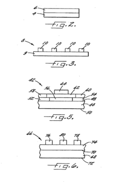
Low micropipe 100 mm silicon carbide wafer
PatentInactiveUS20140291698A1
Innovation
- The development of high-quality silicon carbide wafers with diameters of at least 100 mm and micropipe densities of less than 25 cm^-2, achieved through optimized seeded sublimation growth processes, including careful seed crystal handling, thermal gradient control, and the use of Group III-nitride layers, to reduce defect propagation and maintain polytype identity.
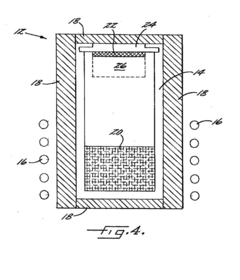
SiC Growth Substrate, CVD Reactor and Method for the Production of SiC
PatentPendingUS20250305140A1
Innovation
- A SiC growth substrate and CVD reactor design that utilizes carbon fiber composite materials and controlled temperature profiles to facilitate high-purity, low-cost production of SiC, minimizing impurities and mechanical stress during crystal growth.
Environmental Impact Assessment of SiC Technology
The integration of Silicon Carbide (SiC) technology in hydroelectric power generation represents a significant advancement with notable environmental implications. When evaluating the environmental impact of SiC wafer technology in this context, several key factors emerge that demonstrate its potential for creating more sustainable energy systems.
SiC-based power electronics significantly reduce energy losses during power conversion processes in hydroelectric facilities. This improved efficiency translates directly to environmental benefits, as the same water resources can generate more electricity, reducing the need for additional dams or water diversion projects that often disrupt aquatic ecosystems. Studies indicate that SiC-based systems can improve conversion efficiency by 15-20% compared to traditional silicon-based technologies.
The manufacturing process of SiC wafers does present certain environmental challenges. Production requires high temperatures exceeding 2000°C, resulting in substantial energy consumption. However, lifecycle assessments reveal that this initial environmental investment is offset by the operational benefits within 1-3 years of deployment in hydroelectric applications, depending on facility scale and utilization patterns.
Water quality preservation represents another significant environmental advantage. Traditional power electronics systems often require extensive cooling mechanisms that may involve water resources and chemical coolants. SiC's superior thermal properties reduce cooling requirements by approximately 30-40%, minimizing thermal pollution in adjacent water bodies and decreasing the risk of coolant leakage into natural water systems.
Carbon footprint reduction constitutes perhaps the most substantial environmental benefit. When implemented across large-scale hydroelectric operations, SiC technology can reduce carbon emissions by an estimated 10-15% compared to conventional systems. This improvement stems from both increased generation efficiency and reduced maintenance requirements, which minimize transportation and replacement part manufacturing emissions over the system lifecycle.
Waste reduction presents another environmental advantage, as SiC components demonstrate significantly longer operational lifespans—typically 2-3 times longer than traditional silicon alternatives. This durability reduces electronic waste generation and the associated environmental impacts of disposal or recycling processes. The extended lifespan also decreases resource consumption for replacement component manufacturing.
Biodiversity protection benefits from SiC implementation as well. The technology's higher efficiency allows hydroelectric facilities to operate effectively with lower water flow rates, potentially reducing the impact on fish migration patterns and riparian ecosystems. Several pilot projects have demonstrated that SiC-equipped facilities can maintain power output while reducing water diversion by 5-10% during critical ecological periods.
Cost-Benefit Analysis of SiC Implementation in Hydropower
The implementation of Silicon Carbide (SiC) technology in hydroelectric power generation systems represents a significant investment that requires thorough economic analysis. Initial capital expenditure for SiC-based power electronics is approximately 2-3 times higher than traditional silicon-based alternatives, with costs ranging from $0.10-0.15 per watt for SiC components compared to $0.04-0.06 for silicon equivalents. However, this premium is offset by substantial operational benefits over the system lifecycle.
Energy efficiency improvements of 2-4% translate to significant revenue increases for hydropower facilities, particularly for large-scale operations where even marginal efficiency gains yield substantial returns. A 100MW facility implementing SiC technology could potentially generate additional annual revenue of $350,000-700,000 based on average electricity prices, depending on capacity factor and market conditions.
Maintenance cost reduction represents another key economic benefit. SiC components demonstrate superior reliability with mean time between failures (MTBF) rates 3-5 times higher than silicon alternatives. This translates to maintenance intervals extending from typical 3-5 year cycles to 10-15 years, reducing both scheduled downtime and associated labor costs by approximately 60-70%.
The thermal management requirements for SiC systems are significantly lower, reducing cooling infrastructure costs by 30-40%. This creates cascading benefits including reduced facility space requirements, lower auxiliary power consumption, and simplified system design. These factors collectively contribute to approximately 15-20% reduction in overall system complexity and associated costs.
Lifecycle analysis indicates that despite higher initial investment, SiC implementations typically achieve break-even within 3-5 years of operation. The total cost of ownership over a 20-year operational period demonstrates 25-35% savings compared to traditional silicon-based systems, with internal rate of return (IRR) calculations showing 15-22% depending on facility scale and operational parameters.
Environmental cost-benefit considerations further strengthen the economic case. Reduced material requirements for cooling systems, higher power density, and longer component lifespans contribute to lower embodied carbon footprints. Additionally, the higher efficiency reduces the environmental impact per kilowatt-hour generated, potentially qualifying facilities for carbon credits or environmental incentives in certain regulatory environments.
Risk assessment indicates that while technology maturity has improved significantly, supply chain vulnerabilities remain a concern. Current global production capacity for SiC wafers is limited, with demand from multiple industries creating potential procurement challenges. Facilities implementing SiC technology should develop robust supply strategies and consider the implications of potential component price volatility in their financial planning.
Unlock deeper insights with Patsnap Eureka Quick Research — get a full tech report to explore trends and direct your research. Try now!
Generate Your Research Report Instantly with AI Agent
Supercharge your innovation with Patsnap Eureka AI Agent Platform!