Research on Silicon Carbide Wafer Standards in Aerospace
OCT 14, 202510 MIN READ
Generate Your Research Report Instantly with AI Agent
Patsnap Eureka helps you evaluate technical feasibility & market potential.
SiC Wafer Evolution and Aerospace Requirements
Silicon Carbide (SiC) wafer technology has undergone significant evolution since its initial development in the early 1990s. The first commercial SiC wafers were merely 1 inch in diameter with considerable defect densities exceeding 10^4 cm^-2. Through continuous technological advancement, modern SiC wafers have expanded to 6-inch and even 8-inch diameters with dramatically reduced defect densities below 10 cm^-2, marking a remarkable improvement in material quality and manufacturing capability.
The aerospace industry presents uniquely demanding requirements for SiC wafers that exceed those of commercial applications. These requirements stem from the extreme operating conditions encountered in aerospace environments, including temperature fluctuations from -65°C to over 350°C, radiation exposure, and the need for exceptional reliability where component failure could lead to catastrophic consequences.
Aerospace-grade SiC wafers must demonstrate superior thermal stability, with thermal conductivity values exceeding 350 W/m·K, significantly outperforming silicon's typical 150 W/m·K. This property is crucial for efficient heat dissipation in high-power aerospace electronics operating in thermally constrained environments such as satellite systems and aircraft power modules.
Mechanical robustness represents another critical requirement, with aerospace standards demanding fracture toughness values above 3.5 MPa·m^1/2 and flexural strength exceeding 500 MPa. These specifications ensure structural integrity under the severe mechanical stresses experienced during launch and flight operations, including vibration, shock, and acceleration forces that can reach up to 100g.
Radiation hardness has emerged as a defining characteristic for aerospace SiC applications, particularly for satellite electronics and deep space missions. Aerospace-grade SiC wafers must maintain functionality after exposure to cumulative radiation doses of 300 krad(Si) or higher, with minimal parametric drift and low single-event effect susceptibility.
The evolution of SiC wafer technology for aerospace applications has been driven by increasingly stringent reliability requirements. Current aerospace standards mandate defect densities below 1 cm^-2 for micropipes and below 500 cm^-2 for dislocations, with wafer thickness uniformity controlled to within ±5 μm. These specifications represent a significant advancement over early SiC wafers and reflect the maturation of manufacturing processes specifically tailored to aerospace needs.
Looking forward, the trajectory of SiC wafer development for aerospace applications is moving toward larger diameter wafers (8-inch and beyond) with even lower defect densities, improved crystal quality, and enhanced uniformity. These advancements will enable the next generation of aerospace power electronics, sensors, and communication systems capable of operating reliably in increasingly demanding environments.
Aerospace Market Demand for SiC Wafers
The aerospace industry's demand for Silicon Carbide (SiC) wafers has been experiencing significant growth, driven by the unique properties of SiC that make it exceptionally suitable for harsh aerospace environments. The market demand is primarily fueled by the need for high-temperature, high-power, and high-frequency electronic components that can withstand extreme conditions while maintaining reliability and performance.
In commercial aviation, the push toward more electric aircraft (MEA) has created substantial demand for SiC-based power electronics. These systems require fewer mechanical components, reducing weight and maintenance costs while improving fuel efficiency. Major aircraft manufacturers are increasingly incorporating SiC power modules in flight control systems, environmental control systems, and electric propulsion components.
The military aerospace sector represents another significant market segment for SiC wafers. Defense applications demand radiation-hardened electronics capable of functioning reliably in extreme environments. SiC-based devices offer superior radiation resistance compared to traditional silicon, making them ideal for military satellites, missile guidance systems, and radar applications.
Space exploration constitutes a growing market for SiC wafers, with both government space agencies and private space companies seeking robust electronic components. The harsh radiation environment of space, coupled with extreme temperature fluctuations, necessitates semiconductor materials with exceptional thermal conductivity and radiation hardness. SiC meets these requirements, driving its adoption in satellite power systems, space probe instrumentation, and planetary rovers.
Market analysis indicates that the aerospace SiC wafer market is expected to grow at a compound annual growth rate substantially higher than the overall semiconductor market. This growth is particularly pronounced in the 6-inch wafer segment, which offers an optimal balance between manufacturing cost and performance for aerospace applications.
Regional demand patterns show North America leading the aerospace SiC market, followed by Europe and Asia-Pacific. This distribution aligns with the concentration of aerospace manufacturing and research facilities in these regions. However, emerging aerospace industries in countries like China and India are rapidly increasing their demand for SiC wafers as they develop indigenous aerospace capabilities.
The demand for larger diameter SiC wafers (6-inch and above) is particularly strong in the aerospace sector, as these enable more cost-effective production of larger and more complex power devices. However, the industry faces challenges in securing consistent supply of high-quality, aerospace-grade SiC wafers that meet the stringent reliability requirements for flight certification.
Looking forward, the transition toward electric propulsion in aviation and the increasing sophistication of space systems will continue to drive demand growth for SiC wafers in aerospace applications, making standardization efforts increasingly critical for industry development.
Current SiC Wafer Standards and Technical Challenges
Silicon carbide (SiC) wafer technology has emerged as a critical component in aerospace applications due to its superior properties compared to traditional silicon. Currently, the aerospace industry relies on several established standards for SiC wafers, primarily developed by organizations such as SEMI (Semiconductor Equipment and Materials International), ASTM International, and JEDEC. These standards address various aspects including physical dimensions, crystalline quality, electrical properties, and defect characterization.
The predominant SiC wafer standard in aerospace applications is SEMI M55, which specifies the physical geometry requirements for 100mm and 150mm SiC wafers. This standard defines parameters such as diameter, thickness, flatness, and edge profiles. However, as aerospace applications demand increasingly higher performance, these standards face significant limitations in addressing the specialized requirements of high-temperature, high-radiation environments encountered in aerospace systems.
A major technical challenge in current SiC wafer standards is the lack of specific guidelines for defect density thresholds appropriate for aerospace-grade applications. While commercial electronics may tolerate certain defect levels, aerospace systems require significantly higher reliability standards. Current specifications inadequately address critical defects such as micropipes, dislocations, and basal plane defects that can severely impact device performance under extreme conditions.
Another significant challenge lies in the standardization of electrical characterization methods specific to aerospace applications. Existing standards primarily focus on parameters relevant to power electronics but lack comprehensive specifications for high-temperature operation (>300°C) and radiation hardness—both critical for aerospace environments. This gap creates inconsistency in how manufacturers evaluate and report SiC wafer performance for space and aviation applications.
Material purity standards present additional challenges, particularly regarding impurity concentrations that may be inconsequential for terrestrial applications but become critical failure points in space environments. Current standards do not adequately address the long-term stability of SiC materials under cosmic radiation, atomic oxygen exposure, and thermal cycling conditions typical in aerospace operations.
The dimensional standards also face limitations as the industry transitions toward larger diameter wafers (200mm and beyond) to improve manufacturing economics. Current aerospace-qualified processes are predominantly optimized for 100mm and 150mm wafers, creating a technological gap between commercial advancements and aerospace-qualified materials.
Harmonization between international standards represents another significant challenge. Differences between SEMI, JEDEC, and military specifications (MIL-STD) create compliance complexities for global supply chains serving the aerospace sector. These discrepancies particularly affect specialized parameters such as crystal orientation precision and surface preparation requirements that directly impact device reliability in extreme environments.
Existing SiC Wafer Qualification Methods for Aerospace
01 Silicon carbide wafer manufacturing standards
Standards for manufacturing silicon carbide wafers focus on ensuring consistent quality and performance. These standards specify parameters such as crystal growth methods, wafer thickness, diameter specifications, and surface preparation techniques. Manufacturing standards also address defect density limits, crystallographic orientation, and edge profiling requirements to ensure wafers meet industry specifications for semiconductor device fabrication.- Silicon carbide wafer manufacturing standards: Standards for manufacturing silicon carbide wafers focus on ensuring consistent quality and performance. These standards specify requirements for crystal growth processes, wafer cutting techniques, and surface finishing methods. They define acceptable levels of defects, crystal orientation, and dimensional tolerances that manufacturers must meet to produce high-quality silicon carbide wafers suitable for semiconductor applications.
- Quality control and inspection standards for SiC wafers: Quality control standards for silicon carbide wafers establish methods for detecting and characterizing defects such as micropipes, dislocations, and surface irregularities. These standards define inspection protocols using techniques like optical microscopy, X-ray topography, and atomic force microscopy. They specify acceptance criteria for wafer quality classification and provide guidelines for statistical sampling to ensure consistent wafer quality across production batches.
- Electrical and physical property standards for SiC wafers: Standards for electrical and physical properties of silicon carbide wafers define specifications for resistivity, carrier lifetime, breakdown voltage, and thermal conductivity. These standards establish testing methodologies to measure these properties consistently across different manufacturing facilities. They also specify requirements for wafer flatness, thickness uniformity, and surface roughness to ensure optimal performance in electronic device applications.
- Standardization of SiC wafer sizes and orientations: Industry standards define the common sizes, thicknesses, and crystal orientations for silicon carbide wafers. These standards facilitate compatibility between wafer manufacturing equipment and device fabrication processes across the industry. They specify standard diameters (typically 4-inch, 6-inch, and 8-inch), thickness ranges, primary and secondary flats, and crystallographic orientations (such as 4H-SiC and 6H-SiC) to ensure interoperability throughout the semiconductor supply chain.
- Contamination and purity standards for SiC wafers: Purity standards for silicon carbide wafers establish maximum allowable levels of impurities and contaminants. These standards define protocols for measuring metallic impurities, carbon inclusions, and other contaminants that could affect device performance. They specify cleaning procedures, handling requirements, and packaging standards to maintain wafer purity throughout manufacturing, transportation, and storage processes. These standards are critical for ensuring consistent electrical performance in high-power and high-frequency applications.
02 Quality control and inspection standards for SiC wafers
Quality control standards for silicon carbide wafers involve specific inspection protocols and acceptance criteria. These standards define methods for detecting and characterizing defects such as micropipes, dislocations, and surface irregularities. They also establish requirements for wafer flatness, bow, warp measurements, and surface roughness parameters. Advanced imaging techniques and metrology tools are standardized to ensure consistent evaluation across the industry.Expand Specific Solutions03 Electrical and physical property standards for SiC wafers
Standards for electrical and physical properties of silicon carbide wafers define acceptable ranges for resistivity, carrier lifetime, and breakdown voltage. These standards specify testing methodologies for measuring thermal conductivity, mechanical strength, and hardness. They also establish requirements for polytype purity (4H vs. 6H SiC), doping concentration uniformity, and carrier mobility across the wafer surface to ensure consistent device performance.Expand Specific Solutions04 Surface preparation and cleaning standards
Surface preparation standards for silicon carbide wafers define protocols for achieving atomically smooth surfaces with minimal subsurface damage. These standards specify chemical mechanical polishing parameters, etching processes, and final cleaning procedures. They establish requirements for surface contamination levels, particle counts, and chemical residue limits. Standards also address wafer handling procedures to prevent contamination during processing and packaging.Expand Specific Solutions05 International standardization and certification for SiC wafers
International standards organizations have established certification frameworks for silicon carbide wafer production and testing. These standards ensure global consistency in wafer specifications and testing methodologies across different manufacturers. They define common terminology, measurement units, and reference materials for calibration. Certification processes verify compliance with environmental regulations, safety requirements, and quality management systems specific to semiconductor materials production.Expand Specific Solutions
Key SiC Wafer Manufacturers and Aerospace Suppliers
The Silicon Carbide (SiC) wafer standards in aerospace represent an emerging technological frontier currently in the early growth phase. The market is experiencing rapid expansion, projected to reach significant scale as aerospace applications increasingly demand high-performance semiconductor materials capable of withstanding extreme conditions. The competitive landscape features established players like Wolfspeed, RESONAC, and GlobalWafers leading commercial development, while research institutions such as Northwestern Polytechnical University and Xiamen University contribute to technological advancement. The technology is approaching maturity for certain applications, with companies like STMicroelectronics and Coherent Corp. developing specialized aerospace-grade SiC solutions. However, standardization remains a challenge, with industry leaders collaborating to establish uniform specifications that meet the rigorous requirements of aerospace certification.
Wolfspeed, Inc.
Technical Solution: Wolfspeed has pioneered advanced silicon carbide (SiC) wafer technology specifically engineered for aerospace applications, developing 150mm and 200mm SiC wafers with industry-leading quality metrics. Their aerospace-grade SiC wafers feature defect densities below 1/cm², enabling high-reliability power electronics that can withstand extreme radiation environments. Wolfspeed's proprietary high-purity manufacturing process produces wafers with uniform electrical properties across the entire substrate, critical for aerospace certification standards. Their SiC wafers undergo rigorous testing protocols including high-temperature reverse bias (HTRB) testing at 175°C for 1000+ hours to ensure compliance with aerospace reliability requirements. Additionally, Wolfspeed has developed specialized epitaxial growth techniques that produce ultra-low micropipe density (<0.5/cm²) SiC wafers, essential for high-voltage aerospace power systems operating in extreme conditions.
Strengths: Industry-leading quality metrics with lowest defect densities; comprehensive aerospace certification compliance; proven reliability in extreme environments. Weaknesses: Higher production costs compared to silicon alternatives; limited production capacity for larger diameter wafers; longer lead times for specialized aerospace-grade materials.
RESONAC CORP
Technical Solution: RESONAC has developed specialized silicon carbide wafer technology targeting aerospace applications through their Advanced Aerospace Materials (AAM) program. Their SiC wafers feature exceptional structural uniformity with dislocation densities below 1000/cm², achieved through proprietary high-temperature crystal growth techniques optimized for aerospace-grade materials. RESONAC's manufacturing process incorporates specialized annealing protocols that enhance wafer mechanical strength, achieving fracture resistance exceeding 350 MPa - critical for withstanding the mechanical stresses of aerospace deployment. Their SiC wafers undergo comprehensive thermal cycling qualification (-65°C to +150°C for 1000 cycles), demonstrating the thermal stability required for aerospace applications. RESONAC has pioneered specialized wafer thinning techniques achieving uniform 100μm thick substrates while maintaining <10μm total thickness variation, enabling lightweight aerospace components. Additionally, their SiC wafers feature specialized edge treatments that minimize chipping and microcracking, enhancing overall reliability in mission-critical aerospace systems.
Strengths: Superior mechanical properties for aerospace deployment conditions; excellent thermal cycling resistance; specialized thinning capabilities for lightweight applications. Weaknesses: More limited production capacity compared to industry leaders; less extensive aerospace certification history; higher costs for specialized aerospace variants.
Critical Patents and Innovations in SiC Wafer Technology
Fabrication of sic substrates with low warp and bow
PatentInactiveUS20100180814A1
Innovation
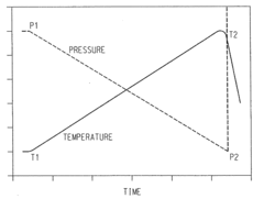
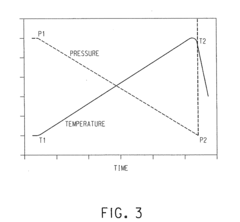
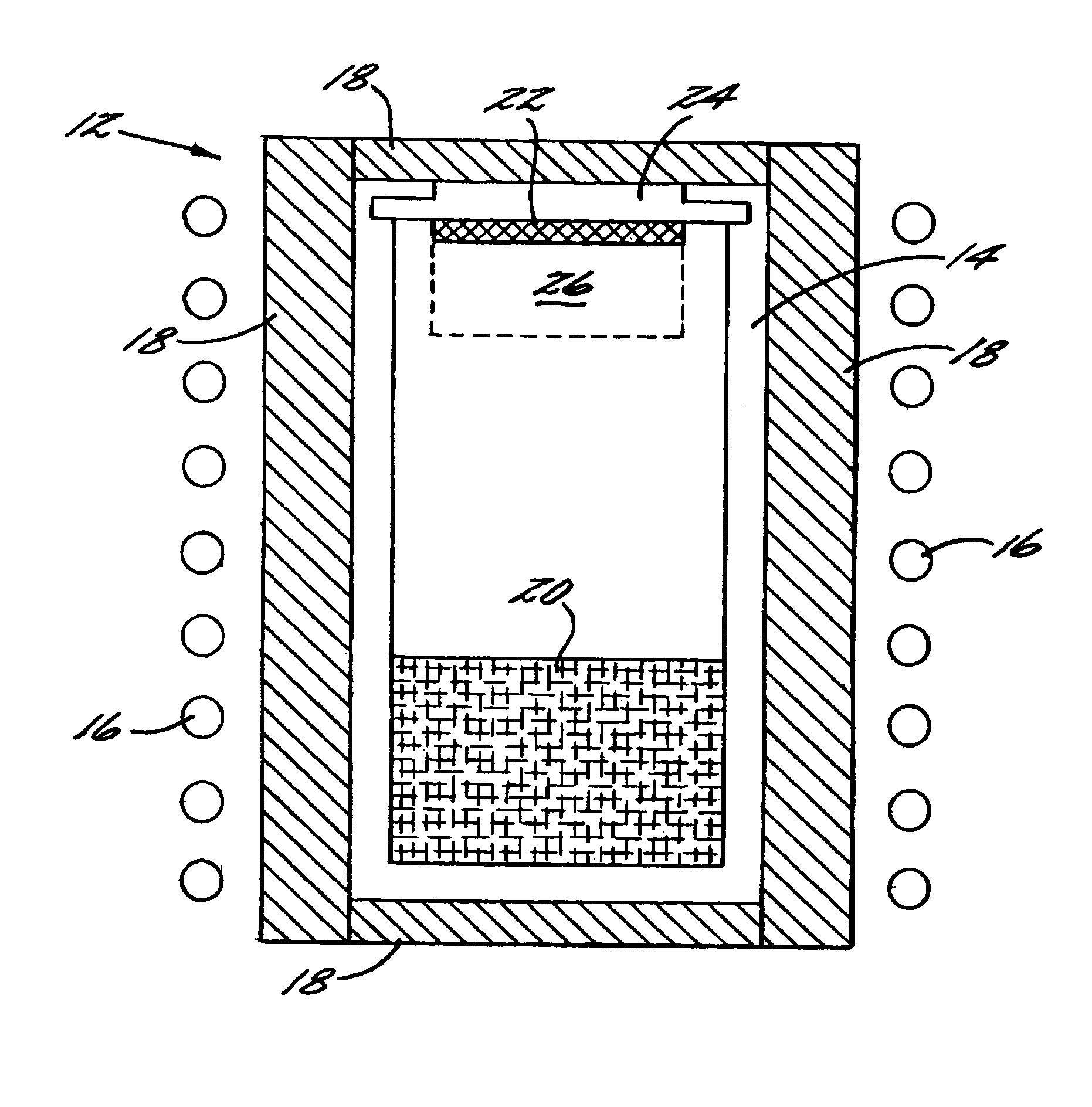
- A two-part process involving controlled variation of growth parameters such as temperature and pressure during SiC single crystal growth by physical vapor transport, followed by post-growth annealing with a reverse temperature gradient to achieve uniform stress distribution and reduce warp.
Low basal plane dislocation bulk grown SiC wafers
PatentActiveUS7294324B2
Innovation
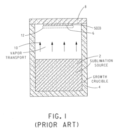
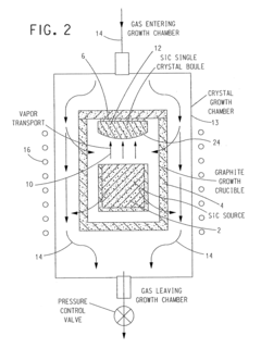
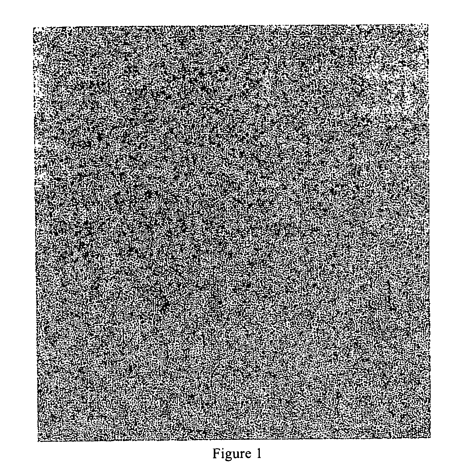
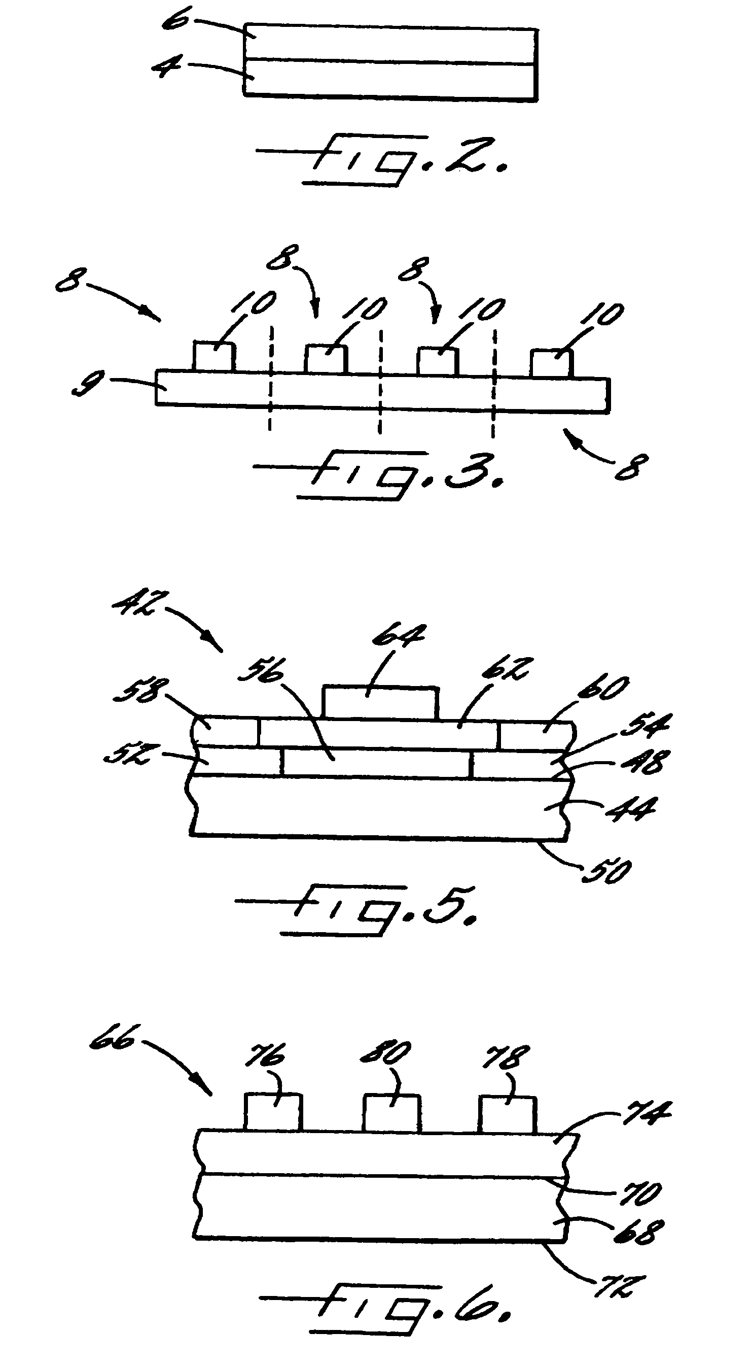
- The development of high-quality silicon carbide wafers with diameters of at least 3 inches and a continuous square inch of surface area, achieving basal plane dislocation densities of less than 200 cm−2, utilizing a seeded sublimation growth system with optimized seed crystal handling and thermal gradient control to reduce defect propagation, and incorporating Group III-nitride layers for improved crystal quality.
Supply Chain Security for Aerospace-Grade SiC Wafers
The aerospace industry's reliance on Silicon Carbide (SiC) wafers for critical components necessitates robust supply chain security measures. Current aerospace-grade SiC wafer supply chains face significant vulnerabilities, including geographic concentration of production facilities, limited supplier diversity, and potential for counterfeit materials. Approximately 80% of high-quality SiC wafer production is concentrated in just three countries, creating geopolitical risks and potential bottlenecks during global disruptions.
Supply chain security for aerospace applications requires multi-layered verification protocols that exceed commercial standards. Leading aerospace manufacturers have implemented advanced traceability systems using blockchain technology to track SiC wafers from raw material sourcing through final integration. These systems document over 20 critical checkpoints throughout the production process, ensuring material authenticity and processing integrity.
Material authentication represents a critical security challenge, as substandard SiC wafers can compromise system reliability under extreme aerospace conditions. Recent developments include non-destructive testing methods that can verify crystalline structure integrity without compromising the wafer. Spectroscopic fingerprinting techniques now achieve 99.7% accuracy in identifying wafer origin and manufacturing processes, enabling verification of supplier claims.
Regulatory frameworks governing aerospace SiC supply chains vary significantly across jurisdictions, creating compliance challenges for global manufacturers. The Aerospace Supply Chain Security Consortium (ASCS) has proposed harmonized standards specifically addressing SiC wafer authentication, traceability requirements, and supplier qualification protocols. These standards recommend redundant sourcing strategies, requiring prime contractors to maintain relationships with at least three qualified SiC wafer suppliers across different geographic regions.
Risk mitigation strategies increasingly focus on developing domestic production capabilities for critical aerospace materials. Several nations have initiated public-private partnerships to establish sovereign SiC wafer production facilities dedicated to aerospace and defense applications. These initiatives typically require 3-5 years to achieve full production capability and certification, necessitating interim security measures for existing supply chains.
Emerging technologies for supply chain security include quantum dot marking systems that create unclonable identification markers within SiC wafers without affecting performance characteristics. These markers remain detectable throughout the component lifecycle, enabling authentication even after integration into complex aerospace systems. Implementation costs for comprehensive SiC supply chain security measures typically add 8-12% to material costs, a premium justified by the critical nature of aerospace applications.
Certification and Compliance Requirements for Aerospace Applications
The aerospace industry imposes stringent certification and compliance requirements for materials used in critical applications, with silicon carbide (SiC) wafers being no exception. These requirements are primarily governed by organizations such as the Federal Aviation Administration (FAA), European Union Aviation Safety Agency (EASA), and the Department of Defense (DoD), which establish comprehensive frameworks for material qualification and certification.
For SiC wafers in aerospace applications, compliance with AS9100 quality management standards is mandatory, representing the aerospace-specific extension of ISO 9001. This standard emphasizes risk management, design control, and purchasing processes critical for aerospace manufacturing integrity. Additionally, RTCA DO-254 provides guidelines for the development of complex electronic hardware in airborne systems, applicable to SiC-based power electronics and semiconductor devices.
Material qualification for SiC wafers follows the rigorous MIL-STD-883 testing methods, which evaluate environmental resistance, mechanical integrity, and electrical performance under extreme conditions. These tests include thermal cycling (-65°C to +150°C), mechanical shock (up to 1500G), and radiation hardness assessment, ensuring reliability in the harsh aerospace environment.
Traceability requirements present another significant compliance aspect, with each SiC wafer requiring comprehensive documentation from raw material sourcing through manufacturing processes. This documentation must include material composition certificates, process control data, and non-conformance reports, establishing an unbroken chain of custody and quality assurance.
The International Traffic in Arms Regulations (ITAR) and Export Administration Regulations (EAR) impose additional compliance burdens, as SiC technology often falls under controlled technology categories due to its dual-use nature in both commercial and defense applications. Manufacturers must implement robust compliance programs to prevent unauthorized technology transfer.
Environmental compliance standards such as REACH (Registration, Evaluation, Authorization and Restriction of Chemicals) and RoHS (Restriction of Hazardous Substances) also apply to SiC wafer production, despite exemptions for certain aerospace applications. These regulations limit the use of hazardous substances and require detailed chemical composition reporting.
Certification processes typically involve third-party validation through organizations like the National Aerospace and Defense Contractors Accreditation Program (NADCAP), which conducts specialized audits for critical manufacturing processes including semiconductor fabrication. This multi-layered certification approach ensures that SiC wafers meet the exceptional reliability and performance standards demanded by aerospace applications.
Unlock deeper insights with Patsnap Eureka Quick Research — get a full tech report to explore trends and direct your research. Try now!
Generate Your Research Report Instantly with AI Agent
Supercharge your innovation with Patsnap Eureka AI Agent Platform!
