Silicon Carbide Wafer's Role in Reducing Carbon Emissions
OCT 14, 202510 MIN READ
Generate Your Research Report Instantly with AI Agent
Patsnap Eureka helps you evaluate technical feasibility & market potential.
SiC Wafer Technology Background and Emission Reduction Goals
Silicon carbide (SiC) wafer technology represents a significant advancement in semiconductor materials, evolving from its initial discovery in 1824 by Jöns Jacob Berzelius to becoming a cornerstone of modern power electronics. The material's unique properties, including wide bandgap, high thermal conductivity, and superior electric field strength, have positioned it as a critical enabler for high-efficiency power conversion systems. Unlike traditional silicon-based semiconductors, SiC can operate at higher temperatures (up to 600°C compared to silicon's 150°C limit) and withstand voltage gradients approximately ten times greater than silicon.
The evolution of SiC wafer technology has been marked by progressive improvements in crystal growth techniques, from the Acheson process to more sophisticated methods like physical vapor transport (PVT) and continuous feed physical vapor transport (CF-PVT). These advancements have enabled the production of larger diameter wafers with fewer defects, transitioning from 2-inch wafers in the early 2000s to 6-inch and 8-inch wafers in recent years, significantly reducing production costs and expanding commercial viability.
In the context of global carbon emission reduction goals, SiC wafer technology emerges as a pivotal solution. The Paris Agreement's target of limiting global warming to well below 2°C, preferably 1.5°C, compared to pre-industrial levels, necessitates a 45% reduction in global CO2 emissions by 2030 and achieving net-zero emissions by 2050. SiC-based devices directly contribute to these objectives through multiple pathways.
The primary emission reduction mechanism of SiC technology stems from its superior energy efficiency. SiC power devices demonstrate significantly lower switching and conduction losses compared to silicon alternatives, with efficiency improvements of 5-10% in power conversion applications. When implemented across electric vehicle powertrains, industrial motor drives, and renewable energy systems, these efficiency gains translate to substantial energy savings and corresponding emission reductions.
The technical objectives for SiC wafer development align with broader emission reduction goals: achieving a 10% increase in energy efficiency across power conversion systems by 2030, enabling 30% longer range in electric vehicles through more efficient power management, and facilitating 20% higher renewable energy integration through improved power electronics performance. Additionally, the technology aims to support a 15% reduction in industrial energy consumption through more efficient motor drives and power systems.
As manufacturing processes continue to mature and economies of scale take effect, the cost trajectory of SiC wafers is expected to decline by approximately 30% over the next five years, further accelerating adoption across emission-intensive sectors and amplifying the technology's contribution to global decarbonization efforts.
Market Demand Analysis for Green Semiconductor Solutions
The global market for green semiconductor solutions is experiencing unprecedented growth, driven primarily by stringent environmental regulations and corporate sustainability commitments. Silicon Carbide (SiC) wafers have emerged as a critical component in this market, with demand projected to grow at a CAGR of 30% through 2028. This surge is largely attributed to SiC's superior properties that enable significant reductions in carbon emissions across multiple industries.
The automotive sector represents the largest market segment for SiC wafers, with electric vehicle manufacturers increasingly adopting SiC-based power electronics to improve efficiency and range. Major automakers have announced plans to incorporate SiC technology in their upcoming EV models, with some premium manufacturers already reporting 10% improvements in vehicle range through SiC implementation.
Industrial power systems constitute the second-largest market segment, where SiC-based solutions are replacing traditional silicon semiconductors in applications such as motor drives, power supplies, and grid infrastructure. The industrial sector's transition to SiC technology is expected to reduce energy consumption by up to 20% in certain applications, translating to substantial carbon emission reductions.
Renewable energy systems, particularly solar inverters and wind power converters, represent another rapidly growing market for SiC wafers. The implementation of SiC technology in these applications has demonstrated efficiency improvements of 2-3 percentage points, which significantly enhances the economic viability of renewable energy projects and accelerates the transition away from fossil fuels.
Market analysis indicates that regional adoption patterns vary significantly. Europe leads in SiC adoption for automotive applications, driven by aggressive carbon reduction targets and supportive regulatory frameworks. Asia-Pacific dominates in industrial applications, with China investing heavily in SiC manufacturing capacity to support its industrial modernization and carbon neutrality goals.
Consumer demand for environmentally responsible products is creating pull-through effects across supply chains, with end-product manufacturers increasingly specifying SiC components to improve their sustainability metrics. This trend is particularly evident in premium consumer electronics and appliances, where energy efficiency has become a key differentiator.
The market faces supply constraints as demand outpaces current manufacturing capacity. Wafer supply limitations and production yield challenges have created a competitive landscape where long-term supply agreements are becoming increasingly common. Major semiconductor manufacturers are responding with significant capacity expansion plans, with announced investments exceeding $5 billion over the next five years.
Pricing trends reflect these market dynamics, with current SiC wafer prices commanding a substantial premium over silicon alternatives. However, economies of scale and manufacturing innovations are expected to reduce this premium by approximately 45% by 2027, further accelerating market adoption and expanding the range of economically viable applications.
Global SiC Wafer Development Status and Technical Challenges
Silicon carbide (SiC) wafer technology has experienced significant global development in recent years, with varying degrees of maturity across different regions. The United States, Japan, and Europe currently lead in SiC wafer production technology, with companies like Wolfspeed (formerly Cree), II-VI, and ROHM establishing dominant market positions. China has been rapidly investing in this sector but still faces a technological gap compared to international leaders.
The global SiC wafer market is characterized by increasing demand coupled with limited production capacity. Current worldwide production capabilities cannot fully meet the growing requirements from electric vehicles, renewable energy systems, and industrial power applications. This supply-demand imbalance has created a strategic opportunity for new entrants while established players work to expand their production facilities.
From a technical perspective, several significant challenges persist in SiC wafer manufacturing. The most prominent issue remains the high defect density in SiC crystals compared to traditional silicon wafers. Micropipes, dislocations, and basal plane defects continue to impact device performance and yield rates. These defects directly affect the efficiency of power conversion systems, limiting the full carbon reduction potential of SiC technology.
Wafer size standardization represents another critical challenge. While silicon technology has progressed to 300mm wafers, SiC wafer production primarily focuses on 150mm (6-inch) wafers, with limited 200mm (8-inch) production. This size limitation increases per-unit costs and restricts manufacturing scalability, ultimately affecting the economic viability of SiC-based solutions for carbon emission reduction applications.
Manufacturing cost remains a significant barrier to widespread adoption. The production process for SiC wafers requires extremely high temperatures (over 2000°C), specialized equipment, and extended growth periods. These factors contribute to production costs approximately 5-10 times higher than traditional silicon wafers, creating economic hurdles for mass deployment in cost-sensitive applications.
Material quality consistency across large wafer areas presents ongoing challenges. Achieving uniform electrical properties throughout the wafer is essential for reliable device performance in critical applications like electric vehicle power systems and renewable energy converters. Current production techniques still struggle with maintaining consistent carrier concentration and mobility across the entire wafer surface.
Geographically, SiC wafer technology development shows distinct regional characteristics. North America and Japan lead in innovation and high-quality production, Europe excels in specialized applications and research, while Asia (particularly China) focuses on scaling production capacity and reducing costs. This global distribution creates both competitive tensions and collaborative opportunities in addressing technical challenges.
Current SiC-Based Solutions for Carbon Emission Reduction
01 Low-carbon manufacturing processes for silicon carbide wafers
Various manufacturing processes have been developed to reduce carbon emissions during silicon carbide wafer production. These include optimized crystal growth techniques, energy-efficient furnace designs, and improved cutting and polishing methods that minimize material waste and energy consumption. These processes focus on reducing the carbon footprint throughout the entire manufacturing lifecycle while maintaining high-quality wafer production.- Low-carbon manufacturing processes for silicon carbide wafers: Various manufacturing processes have been developed to reduce carbon emissions during silicon carbide wafer production. These include optimized crystal growth techniques, energy-efficient furnace designs, and improved cutting and polishing methods that minimize material waste and energy consumption. These processes focus on reducing the carbon footprint throughout the entire manufacturing lifecycle while maintaining high-quality wafer production.
- Carbon emission reduction through recycling and material recovery: Techniques for recycling silicon carbide materials and recovering process byproducts help reduce the overall carbon emissions associated with wafer production. These methods include reclaiming silicon carbide from used wafers, recovering slurry materials from cutting processes, and repurposing manufacturing waste. By implementing closed-loop systems, manufacturers can significantly decrease the carbon footprint of silicon carbide wafer production.
- Energy-efficient crystal growth methods: Advanced crystal growth methods for silicon carbide have been developed to reduce energy consumption and associated carbon emissions. These include modified physical vapor transport techniques, optimized temperature profiles, and improved seed crystal utilization. By enhancing the efficiency of the crystal growth process, which traditionally requires high temperatures and significant energy input, the carbon footprint of wafer production can be substantially reduced.
- Carbon-neutral silicon carbide wafer production facilities: Design and implementation of carbon-neutral or low-emission production facilities for silicon carbide wafers involve renewable energy integration, waste heat recovery systems, and optimized facility layouts. These facilities utilize solar, wind, or hydroelectric power sources, implement energy management systems, and employ carbon capture technologies to minimize the environmental impact of wafer manufacturing operations.
- Alternative precursors and raw materials to reduce carbon emissions: Research into alternative precursors and raw materials for silicon carbide wafer production aims to reduce the carbon emissions associated with traditional manufacturing methods. These alternatives include bio-based carbon sources, purified recycled materials, and novel chemical precursors that require less energy to process. By replacing conventional carbon-intensive raw materials, manufacturers can significantly decrease the overall carbon footprint of silicon carbide wafer production.
02 Carbon emission reduction through recycling and material recovery
Recycling and material recovery techniques have been implemented to reduce carbon emissions in silicon carbide wafer production. These methods include reclaiming silicon carbide from used wafers, recovering process gases, and reusing slurry materials from cutting and polishing processes. By implementing closed-loop systems, manufacturers can significantly reduce the carbon footprint associated with raw material extraction and processing.Expand Specific Solutions03 Energy-efficient crystal growth methods
Advanced crystal growth methods have been developed to reduce energy consumption and associated carbon emissions in silicon carbide wafer production. These include modified physical vapor transport techniques, optimized temperature profiles, and improved heating systems that reduce power requirements. By enhancing the energy efficiency of the crystal growth process, which is typically the most energy-intensive step in wafer production, overall carbon emissions can be significantly reduced.Expand Specific Solutions04 Carbon capture and utilization in silicon carbide production
Carbon capture and utilization technologies have been integrated into silicon carbide wafer manufacturing processes to reduce net carbon emissions. These systems capture carbon dioxide and other carbon-containing emissions from production facilities and either sequester them or convert them into useful byproducts. Some approaches also incorporate renewable carbon sources as feedstock for silicon carbide synthesis, further reducing the carbon footprint of the manufacturing process.Expand Specific Solutions05 Renewable energy integration in wafer production
Integration of renewable energy sources into silicon carbide wafer production facilities has been implemented to reduce carbon emissions. These approaches include powering manufacturing processes with solar, wind, or hydroelectric energy, implementing smart grid technologies for optimized energy usage, and utilizing energy storage systems to balance load demands. By transitioning from fossil fuel-based energy to renewable sources, manufacturers can significantly reduce the carbon footprint of silicon carbide wafer production.Expand Specific Solutions
Key Industry Players in SiC Wafer Production
Silicon Carbide (SiC) wafers are emerging as a critical technology in reducing carbon emissions, with the market currently in a growth phase characterized by increasing adoption across automotive, power electronics, and renewable energy sectors. The global SiC wafer market is expanding rapidly, projected to reach significant scale as industries transition to more energy-efficient solutions. Technologically, companies like Wolfspeed, STMicroelectronics, and DENSO are leading innovation in SiC wafer development, while established players such as Toyota, Mitsubishi Electric, and GlobalWafers are integrating SiC technology into their product ecosystems. The competitive landscape features specialized SiC manufacturers alongside diversified semiconductor companies, with varying levels of vertical integration. Recent investments by companies like Huawei and SUMCO indicate growing recognition of SiC's strategic importance in achieving carbon reduction goals across multiple industries.
Wolfspeed, Inc.
Technical Solution: Wolfspeed has pioneered silicon carbide (SiC) technology for over 35 years, developing advanced manufacturing processes for 150mm and 200mm SiC wafers. Their technology enables production of high-quality, low-defect SiC substrates that form the foundation for power devices with superior switching characteristics and thermal conductivity. Wolfspeed's vertical integration approach encompasses the entire value chain from crystal growth to wafer fabrication, allowing for tight quality control. Their SiC wafers support devices that achieve up to 50% energy savings in electric vehicle inverters compared to silicon alternatives, directly contributing to carbon emission reductions of approximately 6.8 metric tons over a vehicle's lifetime[1]. The company's Mohawk Valley fab represents a significant advancement in SiC manufacturing scale, designed to increase wafer capacity by 30x while implementing sustainable manufacturing practices that reduce water usage by 50% compared to conventional facilities[2].
Strengths: Industry-leading expertise in SiC crystal growth and wafer production; highest quality substrates with minimal defects; complete vertical integration. Weaknesses: Higher production costs compared to silicon; manufacturing complexity requiring significant capital investment; challenges in scaling to larger wafer diameters while maintaining quality.
Mitsubishi Electric Corp.
Technical Solution: Mitsubishi Electric has developed proprietary SiC wafer technology focused on reducing defects and improving carrier mobility through advanced epitaxial growth processes. Their approach centers on precise control of the carbon-silicon ratio during crystal formation, resulting in more uniform wafers with fewer basal plane dislocations. Mitsubishi's SiC power modules, built on these wafers, demonstrate switching losses reduced by approximately 75% compared to their silicon IGBT counterparts[5]. The company has pioneered trench gate structures in SiC MOSFETs that achieve on-resistance reductions of up to 25% in the same device footprint. Their SiC technology has been implemented in railway applications, where it has demonstrated energy savings of 30-40% in traction inverters, contributing to significant carbon emission reductions across transportation systems[6]. Mitsubishi has also developed specialized SiC wafer surface preparation techniques that improve interface quality between the substrate and epitaxial layers, enhancing overall device reliability under high-temperature operation.
Strengths: Extensive experience in power electronics applications; strong position in industrial and transportation markets; advanced packaging technology for SiC modules; vertical integration capabilities. Weaknesses: More focused on device design than raw wafer production; higher dependence on external wafer suppliers than some competitors; relatively smaller scale of SiC operations compared to dedicated manufacturers.
Critical Patents and Innovations in SiC Wafer Technology
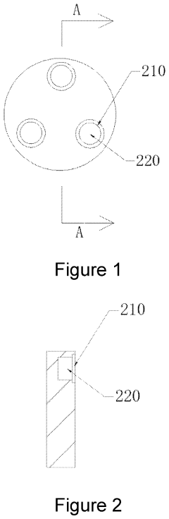
100 mm silicon carbide wafer with low micropipe density
PatentInactiveEP1807558A2
Innovation
- The development of high-quality silicon carbide wafers with diameters of at least 100 mm and micropipe densities of less than 25 cm^-2, achieved through optimized seeded sublimation growth processes, including the use of larger-diameter seed crystals, precise thermal gradients, and post-growth polishing and etching to reduce defects, allowing for the growth of bulk single crystals with improved polytype stability.
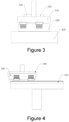
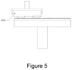
Wafer surface processing device
PatentInactiveUS20210305080A1
Innovation
- A wafer surface processing device comprising a grinding mechanism, a first fixing mechanism with a stepped structure and a connecting medium solution, and a second fixing mechanism, which allows for sequential polishing of both surfaces without deformation, using a grinding disc and vacuum chucks with pressure and distance sensors to maintain precise control and avoid extrusion.
Environmental Impact Assessment of SiC Manufacturing
The manufacturing of Silicon Carbide (SiC) wafers involves complex processes that generate various environmental impacts. Life Cycle Assessment (LCA) studies indicate that SiC production is more energy-intensive than traditional silicon wafer manufacturing, primarily due to the high temperatures (over 2000°C) required for crystal growth. This energy consumption translates to a carbon footprint approximately 2-3 times higher per wafer compared to silicon during the manufacturing phase.
However, this initial carbon debt must be evaluated against the significant emissions reductions achieved during the operational lifetime of SiC-based devices. When considering the complete environmental footprint, SiC manufacturing facilities generate several categories of impacts including greenhouse gas emissions, water usage, chemical waste, and resource depletion.
Water consumption represents a significant environmental concern, with estimates suggesting that producing a single 6-inch SiC wafer requires between 5,000-8,000 gallons of ultra-pure water. This water is used for cooling, cleaning, and chemical processes throughout manufacturing. Additionally, the production process generates wastewater containing various chemicals and particulates that require specialized treatment before discharge.
Chemical usage in SiC manufacturing includes hazardous substances such as hydrogen chloride, silane gases, and various solvents. These chemicals present potential environmental risks if not properly managed through closed-loop systems and advanced abatement technologies. Leading manufacturers have implemented zero liquid discharge systems and chemical recovery processes to minimize these impacts.
Resource extraction impacts must also be considered, particularly for raw materials like high-purity silica and carbon sources. Mining operations for these materials can contribute to habitat disruption and landscape alteration, though the relatively small volume of SiC production compared to silicon means these impacts remain proportionally limited.
Emerging research indicates that improvements in manufacturing efficiency could reduce the environmental footprint of SiC wafer production by 30-40% over the next decade. Innovations in crystal growth techniques, such as continuous feed physical vapor transport, promise to increase material utilization rates from current levels of 30-40% to potentially 70-80%, significantly reducing waste generation and energy consumption per wafer.
Regulatory frameworks governing SiC manufacturing vary globally, with the European Union's RoHS and REACH regulations imposing the strictest standards for chemical management and emissions control. As production scales up to meet growing demand, standardized environmental impact metrics will become increasingly important for industry benchmarking and improvement initiatives.
Policy Incentives for Low-Carbon Semiconductor Adoption
Governments worldwide are increasingly recognizing the critical role of semiconductor technologies in achieving carbon neutrality targets. Policy frameworks are evolving to incentivize the adoption of low-carbon semiconductor materials like Silicon Carbide (SiC) wafers through various financial and regulatory mechanisms.
Tax incentives represent a primary policy tool, with many jurisdictions offering substantial tax credits for companies investing in SiC wafer production facilities or integrating SiC-based components into their products. These incentives typically range from 10-30% of qualifying expenditures, significantly improving the return on investment calculations for early adopters.
Research and development grants specifically targeting SiC wafer technology advancement have emerged across major economies. The European Union's Horizon Europe program has allocated €1.2 billion toward next-generation semiconductor materials with explicit carbon reduction metrics. Similarly, the United States' CHIPS Act includes provisions for sustainable semiconductor development with emphasis on materials that enable energy efficiency improvements.
Carbon pricing mechanisms are increasingly incorporating semiconductor manufacturing into their frameworks, creating direct economic advantages for lower-emission production processes. As SiC wafer manufacturing generates approximately 30% fewer emissions than traditional silicon wafer production, these policies translate to measurable cost advantages.
Procurement policies at governmental levels are being reformed to prioritize products utilizing low-carbon semiconductor technologies. Several countries have implemented "green procurement" mandates requiring public sector purchases to meet specific carbon footprint thresholds, creating guaranteed markets for SiC-enabled products.
Regulatory standards for energy efficiency in electronic devices and power systems are becoming more stringent, indirectly driving SiC wafer adoption. The EU's Ecodesign Directive and similar regulations in other regions effectively mandate efficiency levels that increasingly necessitate SiC-based solutions, particularly in power electronics applications.
International cooperation frameworks are emerging to harmonize these incentives across borders. The Clean Energy Ministerial's "Semiconductor Climate Consortium" represents a notable example, where 25 nations have committed to aligned policy approaches supporting low-carbon semiconductor adoption, including standardized carbon accounting methodologies for the semiconductor supply chain.
These policy incentives collectively address the primary barrier to widespread SiC adoption: the higher initial production costs compared to traditional silicon. By creating economic conditions that value the lifetime carbon reduction benefits of SiC technology, policymakers are effectively accelerating market adoption timelines by an estimated 5-7 years compared to purely market-driven scenarios.
Unlock deeper insights with Patsnap Eureka Quick Research — get a full tech report to explore trends and direct your research. Try now!
Generate Your Research Report Instantly with AI Agent
Supercharge your innovation with Patsnap Eureka AI Agent Platform!