Research on Silicon Carbide Wafer Growth Techniques
OCT 14, 20259 MIN READ
Generate Your Research Report Instantly with AI Agent
Patsnap Eureka helps you evaluate technical feasibility & market potential.
SiC Wafer Technology Background and Objectives
Silicon Carbide (SiC) has emerged as a revolutionary semiconductor material over the past several decades, evolving from its initial discovery in 1824 by Jöns Jacob Berzelius to becoming a cornerstone of next-generation power electronics. The development trajectory of SiC wafer technology has been characterized by persistent efforts to overcome significant technical challenges in crystal growth, particularly in achieving larger diameters and higher quality substrates.
The historical progression of SiC wafer technology began with small-diameter crystals in the 1950s, followed by the introduction of the modified Lely method in the 1970s, which represented the first significant breakthrough in controlled SiC crystal growth. The 1980s and 1990s witnessed the development of the Physical Vapor Transport (PVT) method, establishing the foundation for commercial SiC wafer production.
Current technological trends indicate a clear movement toward larger wafer diameters, with industry standards evolving from 2-inch to 4-inch, 6-inch, and now pushing toward 8-inch wafers. This scaling is critical for reducing production costs and increasing device yield, making SiC more competitive with traditional silicon-based technologies.
Parallel to diameter expansion, significant emphasis has been placed on defect reduction, particularly addressing micropipes, dislocations, and basal plane defects that compromise device performance. The industry has witnessed remarkable progress, with defect densities decreasing by several orders of magnitude over the past two decades.
The primary technical objectives in SiC wafer growth research center on several key areas. First, achieving consistent production of larger diameter wafers (8-inch and beyond) while maintaining structural integrity and crystal quality. Second, further reducing defect densities to approach theoretical limits, particularly targeting zero micropipe density. Third, increasing growth rates to improve production economics without sacrificing material quality.
Additionally, researchers aim to enhance polytype control, focusing primarily on 4H-SiC for power applications, while exploring specialized applications for other polytypes. Improving wafer uniformity in terms of thickness, resistivity, and dopant distribution represents another critical objective, as these parameters directly impact device performance consistency.
The ultimate goal of current SiC wafer technology development is to establish manufacturing processes capable of producing high-quality, large-diameter wafers at costs that enable broader market adoption across power electronics, electric vehicles, renewable energy systems, and emerging applications in harsh environment electronics and high-frequency communications.
Market Analysis for SiC Wafer Applications
The Silicon Carbide (SiC) wafer market has experienced significant growth in recent years, primarily driven by the increasing demand for high-power and high-frequency electronic devices. The global SiC wafer market was valued at approximately $420 million in 2020 and is projected to reach $1.5 billion by 2027, representing a compound annual growth rate (CAGR) of around 19.8% during this forecast period.
Power electronics represents the largest application segment for SiC wafers, accounting for over 60% of the total market share. This dominance is attributed to SiC's superior properties compared to traditional silicon, including higher breakdown electric field strength, thermal conductivity, and electron saturation velocity. These characteristics make SiC ideal for high-voltage, high-temperature, and high-frequency applications.
The automotive sector has emerged as a key growth driver for SiC wafers, particularly in electric vehicles (EVs) and hybrid electric vehicles (HEVs). SiC-based power modules in EV inverters can reduce power losses by up to 80% compared to silicon-based alternatives, extending vehicle range and reducing battery requirements. Major automotive manufacturers including Tesla, BMW, and Toyota have already incorporated SiC power electronics in their EV models.
Industrial applications constitute another significant market segment, with SiC wafers being increasingly utilized in motor drives, power supplies, and renewable energy systems. In solar inverters, SiC devices can improve efficiency by 1-3 percentage points, which translates to substantial energy savings over the lifetime of the system.
The telecommunications industry represents an emerging application area for SiC wafers, particularly in 5G infrastructure. SiC-based RF devices offer higher power density and efficiency for base station transmitters, addressing the increased power requirements of next-generation wireless networks.
Regionally, Asia-Pacific dominates the SiC wafer market, accounting for approximately 45% of global consumption, with China, Japan, and South Korea being the major contributors. North America follows with around 30% market share, driven by defense applications and the growing EV market. Europe represents about 20% of the market, with strong growth in automotive and industrial sectors.
The market is characterized by supply constraints, with demand consistently exceeding available production capacity. This imbalance has resulted in premium pricing for SiC wafers compared to silicon alternatives, with 6-inch SiC wafers typically commanding 10-15 times the price of equivalent silicon wafers. However, as manufacturing technologies mature and economies of scale improve, prices are expected to decrease, further accelerating market adoption across various applications.
Global SiC Crystal Growth Technical Challenges
Silicon carbide (SiC) crystal growth faces significant technical challenges that have hindered widespread commercialization despite its superior material properties. The primary obstacle remains the difficulty in growing large-diameter, high-quality single crystals with minimal defects. The physical vapor transport (PVT) method, while dominant in commercial production, struggles with thermal gradient control across larger diameters, resulting in increased stress and defect formation.
Micropipe defects, though reduced in recent years, continue to plague SiC wafers, particularly at diameters exceeding 150mm. These hollow core screw dislocations propagate through the crystal during growth and severely impact device performance. Current industry leaders report micropipe densities below 1 cm^-2, but achieving zero-micropipe material consistently at commercial scale remains elusive.
Polytype control presents another fundamental challenge. SiC exists in over 200 polytypes with 4H-SiC preferred for power electronics due to its wider bandgap and higher electron mobility. However, maintaining polytype stability during growth requires precise temperature and pressure control, as unwanted polytype inclusions create performance-degrading heterojunctions within devices.
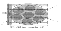
Thermal management during crystal growth creates significant engineering difficulties. The extreme temperatures required (typically 2000-2500°C) accelerate crucible degradation and introduce impurities. Graphite crucibles, while standard, gradually release carbon particles that become incorporated as defects. Alternative crucible materials that can withstand these conditions while remaining chemically inert are limited.
Scaling to larger diameters (200mm and beyond) compounds these challenges exponentially. The semiconductor industry's push toward larger wafers for economic manufacturing encounters fundamental physical limitations in SiC growth. Maintaining uniform thermal fields across larger diameters requires sophisticated heating designs and simulation-guided growth processes that many manufacturers struggle to perfect.
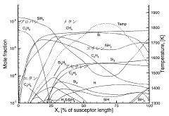
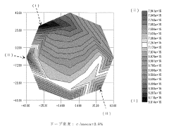
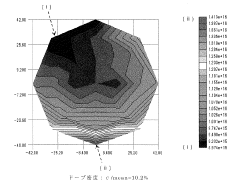
Doping uniformity across the wafer presents additional complications. Achieving consistent electrical properties throughout the crystal requires precise control of dopant incorporation during growth. Nitrogen (n-type) and aluminum (p-type) doping often exhibit radial and axial variations that complicate device manufacturing and reduce yield.
Surface polishing and preparation after crystal growth introduce further challenges. SiC's extreme hardness (9.5 on Mohs scale) makes conventional polishing techniques ineffective. Chemical-mechanical polishing processes must be carefully optimized to remove subsurface damage without introducing new defects, a process that becomes increasingly difficult with larger wafer sizes.
These technical hurdles collectively contribute to the high cost of SiC wafers compared to silicon alternatives, limiting broader adoption despite SiC's superior performance characteristics in power electronics applications.
Micropipe defects, though reduced in recent years, continue to plague SiC wafers, particularly at diameters exceeding 150mm. These hollow core screw dislocations propagate through the crystal during growth and severely impact device performance. Current industry leaders report micropipe densities below 1 cm^-2, but achieving zero-micropipe material consistently at commercial scale remains elusive.
Polytype control presents another fundamental challenge. SiC exists in over 200 polytypes with 4H-SiC preferred for power electronics due to its wider bandgap and higher electron mobility. However, maintaining polytype stability during growth requires precise temperature and pressure control, as unwanted polytype inclusions create performance-degrading heterojunctions within devices.
Thermal management during crystal growth creates significant engineering difficulties. The extreme temperatures required (typically 2000-2500°C) accelerate crucible degradation and introduce impurities. Graphite crucibles, while standard, gradually release carbon particles that become incorporated as defects. Alternative crucible materials that can withstand these conditions while remaining chemically inert are limited.
Scaling to larger diameters (200mm and beyond) compounds these challenges exponentially. The semiconductor industry's push toward larger wafers for economic manufacturing encounters fundamental physical limitations in SiC growth. Maintaining uniform thermal fields across larger diameters requires sophisticated heating designs and simulation-guided growth processes that many manufacturers struggle to perfect.
Doping uniformity across the wafer presents additional complications. Achieving consistent electrical properties throughout the crystal requires precise control of dopant incorporation during growth. Nitrogen (n-type) and aluminum (p-type) doping often exhibit radial and axial variations that complicate device manufacturing and reduce yield.
Surface polishing and preparation after crystal growth introduce further challenges. SiC's extreme hardness (9.5 on Mohs scale) makes conventional polishing techniques ineffective. Chemical-mechanical polishing processes must be carefully optimized to remove subsurface damage without introducing new defects, a process that becomes increasingly difficult with larger wafer sizes.
These technical hurdles collectively contribute to the high cost of SiC wafers compared to silicon alternatives, limiting broader adoption despite SiC's superior performance characteristics in power electronics applications.
Current SiC Crystal Growth Methods Comparison
01 Silicon Carbide Wafer Manufacturing Methods
Various methods for manufacturing silicon carbide wafers have been developed to improve quality and yield. These methods include specialized crystal growth techniques, wafer slicing processes, and surface preparation methods. Advanced manufacturing approaches help reduce defects and improve the crystalline structure of SiC wafers, which is crucial for high-performance semiconductor applications.- Silicon Carbide Wafer Manufacturing Methods: Various methods for manufacturing silicon carbide wafers have been developed to improve quality and yield. These methods include specific crystal growth techniques, wafer slicing processes, and surface preparation methods. Advanced manufacturing techniques help to reduce defects and improve the crystalline structure of the wafers, making them suitable for high-performance electronic applications.
- Defect Reduction in Silicon Carbide Wafers: Techniques for reducing defects in silicon carbide wafers are crucial for improving device performance. These include methods to minimize micropipes, dislocations, and other crystallographic defects that can affect electrical properties. Processes such as high-temperature annealing, specialized polishing techniques, and defect passivation methods help to enhance the overall quality and reliability of silicon carbide wafers for semiconductor applications.
- Surface Treatment and Polishing of Silicon Carbide Wafers: Surface treatment and polishing processes are essential for preparing silicon carbide wafers for device fabrication. These processes include chemical-mechanical polishing, plasma etching, and thermal oxidation to achieve atomically smooth surfaces with minimal subsurface damage. Advanced surface treatments help to improve wafer flatness, reduce roughness, and remove contaminants, resulting in better device performance and yield.
- Epitaxial Growth on Silicon Carbide Substrates: Epitaxial growth processes on silicon carbide substrates are used to create high-quality semiconductor layers for device fabrication. These processes involve the controlled deposition of thin crystalline layers on silicon carbide wafers using techniques such as chemical vapor deposition. The epitaxial layers can be tailored for specific device requirements, enabling the development of high-performance power electronics, RF devices, and sensors.
- Silicon Carbide Wafer Applications in Power Electronics: Silicon carbide wafers are increasingly used in power electronics applications due to their superior properties compared to traditional silicon. These applications include high-voltage power devices, electric vehicle components, renewable energy systems, and industrial motor drives. The wide bandgap, high thermal conductivity, and high breakdown field strength of silicon carbide enable the development of more efficient and compact power electronic systems that can operate at higher temperatures and frequencies.
02 Defect Reduction Techniques in SiC Wafers
Techniques for reducing defects in silicon carbide wafers are essential for improving device performance. These include methods for minimizing micropipes, dislocations, and other crystallographic defects that can affect electrical properties. Processes such as thermal annealing, epitaxial growth optimization, and specialized polishing techniques help achieve higher quality wafers with fewer defects.Expand Specific Solutions03 Surface Treatment and Polishing of SiC Wafers
Surface treatment and polishing methods are critical for preparing silicon carbide wafers for device fabrication. These processes include chemical-mechanical polishing, plasma etching, and other techniques to achieve atomically smooth surfaces with minimal subsurface damage. Proper surface preparation ensures better device performance and reliability in the final semiconductor products.Expand Specific Solutions04 Epitaxial Growth on SiC Substrates
Epitaxial growth techniques on silicon carbide substrates are used to create high-quality semiconductor layers for device fabrication. These methods include chemical vapor deposition (CVD) and other growth processes optimized for the unique properties of SiC. Controlling parameters such as temperature, pressure, and gas flow enables the growth of uniform epitaxial layers with desired electrical characteristics.Expand Specific Solutions05 Large Diameter SiC Wafer Development
Development of large diameter silicon carbide wafers is a significant focus area to reduce manufacturing costs and increase production efficiency. Techniques for growing larger SiC boules and processing them into wafers with consistent properties throughout the diameter present unique challenges. Innovations in crystal growth, handling, and processing enable the production of larger wafers while maintaining quality and performance characteristics.Expand Specific Solutions
Leading SiC Wafer Manufacturers and Competitors
The Silicon Carbide (SiC) wafer growth technology market is currently in a growth phase, transitioning from early adoption to mainstream implementation, with an estimated market size exceeding $2 billion and projected strong annual growth rates of 15-20%. The competitive landscape features established leaders like Wolfspeed and RESONAC alongside emerging players such as TanKeBlue and Jiangsu Tankeblue Semiconductor. Technology maturity varies significantly across competitors, with companies like Wolfspeed, Sumitomo Electric, and GlobalWafers demonstrating advanced capabilities in producing larger diameter wafers (6-8 inch) with lower defect densities, while newer entrants from China (TanKeBlue, Hunan Sanan) are rapidly advancing their technical capabilities through significant R&D investments and government support to close the technology gap.
Wolfspeed, Inc.
Technical Solution: Wolfspeed has pioneered advanced SiC wafer growth techniques using physical vapor transport (PVT) method with proprietary high-temperature crystal growth furnaces. Their technology enables the production of 150mm and 200mm SiC wafers with industry-leading quality metrics. Wolfspeed's approach involves precise control of thermal gradients during crystal growth, resulting in reduced defect densities below 1 defect/cm² in their premium wafers. The company has developed specialized seed crystal preparation techniques and post-growth processes including precision wafering, chemical mechanical polishing (CMP), and advanced metrology systems to ensure wafer uniformity. Their recent innovations include the Zero-Micropipe technology and implementation of AI-driven process control systems that have improved yield rates by approximately 25% while reducing production cycle times.
Strengths: Industry-leading quality with lowest defect densities; advanced manufacturing scale with 200mm capability; vertically integrated business model from substrate to device manufacturing. Weaknesses: Higher production costs compared to silicon; limited production capacity relative to growing market demand; challenges in scaling to larger diameter wafers while maintaining quality.
RESONAC CORP
Technical Solution: RESONAC (formerly Showa Denko) has developed a proprietary High-Temperature Chemical Vapor Deposition (HTCVD) technique for SiC wafer production, differentiating from the conventional PVT method. Their process utilizes specialized gas-phase chemistry to grow high-purity SiC crystals at temperatures exceeding 2000°C. RESONAC's approach enables precise control of dopant concentrations and reduces certain types of crystal defects by approximately 40% compared to traditional methods. The company has successfully commercialized 150mm SiC wafers and is developing 200mm technology with enhanced uniformity parameters. Their manufacturing process incorporates advanced in-situ monitoring systems that allow real-time adjustments to growth conditions, resulting in wafers with resistivity variations of less than 10% across the entire substrate. RESONAC has also pioneered techniques to reduce basal plane dislocations, which are critical for high-voltage device performance.
Strengths: Unique HTCVD technology offering potentially lower defect densities; excellent dopant control and uniformity; strong integration with downstream device manufacturing. Weaknesses: Smaller production scale compared to market leaders; higher energy consumption in manufacturing process; more complex equipment requirements for the HTCVD approach.
Key Patents in SiC Wafer Defect Reduction
Silicon carbide epitaxial growth system and manufacturing method of silicon carbide epitaxial wafer
PatentActiveJP2021015896A
Innovation
- A silicon carbide epitaxial growth apparatus and method that incorporates a tantalum carbide member on the outer peripheral side of the wafer holder to suppress nitrogen deposition and maintain uniform carrier concentration during epitaxial growth, using a thermal chemical vapor deposition method.
Silicon carbide epitaxial growth method
PatentActiveJP2018046085A
Innovation
- The method involves using a mixed gas composition of hydrocarbon raw material gases with controlled C/Si ratios, including methane and acetylene or ethylene and ethane, within specific volume percentages, to ensure uniform doping density by optimizing the decomposition behavior of hydrocarbon gases during epitaxial growth.
Supply Chain Analysis for SiC Wafer Materials
The silicon carbide (SiC) wafer supply chain represents a complex ecosystem of raw materials, processing technologies, and distribution networks that are critical to the advancement of SiC wafer growth techniques. The supply chain begins with the sourcing of high-purity silicon and carbon, typically in the form of silica sand and petroleum coke or rice husks, which must meet stringent quality requirements for semiconductor applications.
Primary processing involves the synthesis of SiC powder through various methods, including the Acheson process and chemical vapor deposition (CVD). These processes require specialized equipment and expertise, creating a significant barrier to entry for new market participants. The global distribution of these capabilities is concentrated in a few regions, primarily Japan, the United States, and Europe.
The transformation of SiC powder into single crystal ingots represents a critical bottleneck in the supply chain. This process demands ultra-high temperature furnaces operating at over 2000°C and precise control systems. Currently, only a limited number of manufacturers possess the technical capability to produce high-quality SiC ingots at commercial scale, leading to supply constraints as demand increases.
Wafer processing stages, including slicing, lapping, polishing, and cleaning, require specialized equipment that differs significantly from traditional silicon wafer processing tools. The extreme hardness of SiC (9.5 on the Mohs scale) necessitates diamond-based cutting and polishing technologies, which are capital-intensive and technically challenging to optimize.
Supply chain vulnerabilities exist in several areas, particularly in the dependency on specialized equipment manufacturers and the limited number of qualified suppliers for high-purity raw materials. The COVID-19 pandemic exposed these vulnerabilities, with disruptions in global logistics causing delays in equipment delivery and raw material availability.
Pricing dynamics within the SiC wafer supply chain reflect these constraints, with SiC wafers commanding prices 5-10 times higher than comparable silicon wafers. However, economies of scale and technological improvements are gradually reducing these cost differentials, with projections suggesting a 30-40% cost reduction over the next five years as production volumes increase.
Sustainability considerations are becoming increasingly important in the SiC supply chain, with manufacturers exploring more energy-efficient growth techniques and environmentally friendly processing methods. The energy-intensive nature of SiC production presents both a challenge and an opportunity for innovation in sustainable manufacturing practices.
Environmental Impact of SiC Manufacturing Processes
The manufacturing of Silicon Carbide (SiC) wafers involves complex processes that generate significant environmental impacts across multiple dimensions. The high-temperature synthesis required for SiC crystal growth, typically exceeding 2000°C, results in substantial energy consumption, primarily from electricity usage in furnaces. This energy-intensive nature contributes considerably to greenhouse gas emissions, with estimates suggesting that producing a single 6-inch SiC wafer may generate between 600-900 kg of CO2 equivalent emissions, significantly higher than comparable silicon wafer production.
Water usage represents another critical environmental concern, as SiC manufacturing requires ultra-pure water for cleaning and processing steps. A typical SiC wafer fabrication facility may consume 5-7 million gallons of water daily, with much of this water containing dissolved chemicals and particulates requiring specialized treatment before discharge. The industry has begun implementing closed-loop water recycling systems, though adoption remains inconsistent across manufacturers.
Chemical usage in SiC production presents additional environmental challenges. The process utilizes hazardous substances including silane gases, hydrogen chloride, and various metallic dopants. These chemicals require careful handling and disposal protocols to prevent air and water contamination. Particularly concerning is the use of chlorinated compounds in certain SiC growth techniques, which can potentially contribute to ozone depletion if released.
Solid waste generation from SiC manufacturing includes silicon carbide particulates, spent polishing compounds, and damaged wafers. These materials often contain trace amounts of dopants and metals that complicate disposal. Industry data suggests that for every kilogram of finished SiC wafer, approximately 2-3 kilograms of solid waste may be generated throughout the production process.
Recent technological innovations are addressing these environmental concerns through several approaches. Advanced furnace designs with improved thermal efficiency have reduced energy consumption by 15-20% compared to older systems. Alternative growth methods like Halide Chemical Vapor Deposition (HCVD) demonstrate lower resource intensity than traditional Physical Vapor Transport (PVT) techniques. Additionally, manufacturers are increasingly implementing ISO 14001 environmental management systems and participating in sustainability reporting initiatives.
The regulatory landscape surrounding SiC manufacturing continues to evolve, with stricter emissions standards and chemical usage restrictions being implemented in major manufacturing regions. Companies leading in environmental performance are finding competitive advantages through reduced compliance costs and improved stakeholder relations, suggesting that environmental considerations will increasingly influence the industry's technological development trajectory.
Unlock deeper insights with Patsnap Eureka Quick Research — get a full tech report to explore trends and direct your research. Try now!
Generate Your Research Report Instantly with AI Agent
Supercharge your innovation with Patsnap Eureka AI Agent Platform!