

Silicon Carbide Wafer Surface Engineering for Optoelectronics
OCT 14, 20259 MIN READ
Generate Your Research Report Instantly with AI Agent
Patsnap Eureka helps you evaluate technical feasibility & market potential.
SiC Wafer Technology Background and Objectives
Silicon Carbide (SiC) has emerged as a revolutionary semiconductor material for optoelectronic applications, offering exceptional thermal conductivity, high breakdown electric field strength, and wide bandgap properties. The evolution of SiC wafer technology spans several decades, beginning with rudimentary crystal growth techniques in the 1950s and advancing to sophisticated epitaxial growth methods in the 21st century. This technological progression has been driven by increasing demands for high-performance electronic devices capable of operating under extreme conditions.
The historical trajectory of SiC wafer development reveals significant milestones, including the commercialization of 2-inch wafers in the 1990s, followed by 4-inch wafers in the early 2000s, and more recently, the introduction of 6-inch and 8-inch wafers. Each advancement has substantially reduced production costs while improving material quality, thereby expanding potential applications across various industries.
Current SiC wafer technology faces persistent challenges related to surface engineering, particularly in achieving atomically smooth surfaces with minimal defects. These surface characteristics are critical for optoelectronic applications where interface quality directly impacts device performance. Traditional mechanical polishing techniques have proven insufficient for meeting the stringent requirements of modern optoelectronic devices, necessitating innovative approaches to surface preparation.
The global market for SiC-based optoelectronic devices is projected to grow at a compound annual growth rate exceeding 25% through 2030, driven primarily by applications in power electronics, automotive systems, and renewable energy infrastructure. This market expansion underscores the strategic importance of advancing SiC wafer surface engineering technologies.
The primary technical objectives for SiC wafer surface engineering in optoelectronic applications include: reducing surface roughness to sub-nanometer levels, minimizing subsurface damage, controlling surface termination for optimal electronic properties, developing scalable and cost-effective polishing techniques, and establishing standardized characterization methodologies for surface quality assessment.
Achieving these objectives requires interdisciplinary collaboration across materials science, chemical engineering, and semiconductor physics. Recent research indicates promising directions in chemical-mechanical polishing (CMP) techniques, plasma-assisted etching, and high-temperature hydrogen etching for surface preparation. These approaches aim to overcome the inherent hardness and chemical inertness of SiC that have historically complicated surface engineering efforts.
The successful development of advanced SiC wafer surface engineering techniques is expected to enable next-generation optoelectronic devices with superior performance characteristics, including higher efficiency, greater reliability, and extended operational lifetimes in harsh environments. These improvements align with broader industry trends toward energy efficiency, miniaturization, and enhanced functionality in electronic systems.
Market Analysis for SiC-Based Optoelectronic Devices
The global market for SiC-based optoelectronic devices is experiencing robust growth, driven by increasing demand for high-performance electronic components in power electronics, automotive, telecommunications, and aerospace industries. The market value reached approximately $1.2 billion in 2022 and is projected to grow at a compound annual growth rate (CAGR) of 18.3% through 2028, potentially reaching $3.9 billion by the end of the forecast period.
Silicon carbide's unique properties—wide bandgap, high thermal conductivity, and excellent chemical stability—make it particularly valuable for optoelectronic applications operating in harsh environments. The automotive sector represents the largest market segment, accounting for nearly 35% of total demand, primarily for electric vehicle power electronics and LED lighting systems that require superior thermal management.
Regional analysis indicates that Asia-Pacific currently dominates the market with approximately 45% share, led by manufacturing powerhouses in Japan, South Korea, and China. North America follows with 28% market share, while Europe accounts for 22%. The remaining 5% is distributed across other regions. China's aggressive investments in semiconductor manufacturing capabilities are expected to significantly alter this distribution over the next five years.
Consumer electronics applications are showing the fastest growth rate at 22.4% annually, as manufacturers increasingly adopt SiC-based components for high-efficiency power management systems and display technologies. The telecommunications sector is also rapidly expanding its utilization of SiC optoelectronics for 5G infrastructure deployment, with particular emphasis on high-frequency, high-power applications.
Market penetration faces challenges related to production costs, which remain 2.5-3 times higher than traditional silicon-based alternatives. However, economies of scale and manufacturing innovations are gradually reducing this gap. Industry analysts predict price parity for certain applications could be achieved by 2027, potentially triggering accelerated market adoption.
Supply chain considerations reveal potential vulnerabilities, with 70% of high-purity SiC wafer production concentrated among just five global suppliers. Recent geopolitical tensions and pandemic-related disruptions have prompted manufacturers to pursue supply chain diversification strategies, including development of regional production capabilities and long-term supplier agreements.
Emerging applications in quantum computing, biomedical sensors, and aerospace systems represent significant growth opportunities, with these sectors expected to collectively contribute an additional $500 million to market value by 2030. Venture capital investments in SiC optoelectronics startups have surged, with funding rounds totaling $780 million in 2022 alone, indicating strong confidence in future market expansion.
Current Challenges in SiC Surface Engineering
Despite significant advancements in Silicon Carbide (SiC) technology, surface engineering for optoelectronic applications faces several critical challenges that impede widespread commercial adoption. The primary obstacle remains the high density of surface defects, particularly micropipes and basal plane dislocations, which significantly impact device performance and reliability. These defects create recombination centers that reduce quantum efficiency and increase leakage current in optoelectronic devices, ultimately limiting their operational lifetime.
Surface roughness presents another substantial challenge, with typical as-cut SiC wafers exhibiting RMS roughness values of 5-10 nm, significantly higher than the sub-nanometer requirements for high-performance optoelectronic applications. Current chemical-mechanical polishing (CMP) techniques struggle to achieve consistent sub-nanometer roughness across large-diameter wafers without introducing subsurface damage.
The presence of surface contaminants, including metallic impurities and carbon residues from processing steps, continues to plague SiC surface preparation. These contaminants can alter the electronic properties of the surface, creating unwanted energy states that interfere with optical emission and absorption processes critical for optoelectronic functionality.
Interface engineering between SiC and deposited materials represents a significant technical hurdle. The formation of stable, low-defect interfaces is essential for efficient carrier transport and optical coupling. Current deposition techniques often result in interface states that trap carriers and reduce device efficiency, particularly at the SiC/dielectric interfaces crucial for device isolation and passivation.
Surface charge management remains problematic, with SiC surfaces exhibiting high densities of fixed charges that can reach 10^12 cm^-2. These charges distort band alignment and create unpredictable electric fields that compromise device performance consistency. Existing passivation techniques have shown limited success in neutralizing these charges without introducing additional defects.
The challenge of achieving atomically flat, step-controlled surfaces necessary for epitaxial growth of optoelectronic structures persists. Current hydrogen etching techniques produce terraces with inconsistent widths and heights, leading to non-uniform epitaxial layers that compromise device performance and yield.
Temperature stability of surface treatments presents another significant obstacle. Many surface passivation and functionalization methods degrade at the high operating temperatures typical for SiC devices (>200°C), resulting in progressive performance deterioration during device operation. This thermal instability limits the long-term reliability of SiC-based optoelectronic systems in demanding applications.
Current Surface Engineering Solutions for SiC Wafers
01 Surface polishing and planarization techniques
Various methods for polishing and planarizing silicon carbide wafer surfaces to achieve atomically flat surfaces with minimal defects. These techniques include chemical mechanical polishing (CMP), mechanical polishing with diamond slurries, and specialized etching processes that can remove surface damage while maintaining crystalline integrity. These processes are critical for subsequent device fabrication and can significantly improve electrical performance of SiC-based devices.- Surface polishing and planarization techniques: Various methods for polishing and planarizing silicon carbide wafer surfaces to achieve atomically flat surfaces with minimal defects. These techniques include chemical-mechanical polishing (CMP), plasma-assisted polishing, and specialized abrasive processes that can effectively remove surface irregularities while minimizing subsurface damage. The planarization processes are critical for subsequent device fabrication and can significantly improve the electrical and thermal properties of devices built on these wafers.
- Defect reduction and surface preparation methods: Techniques focused on reducing surface defects such as micropipes, dislocations, and scratches on silicon carbide wafers. These methods include specialized etching processes, thermal treatments, and surface conditioning techniques that can effectively remove or passivate defects. Surface preparation methods are designed to create optimal conditions for epitaxial growth and device fabrication, resulting in improved yield and performance of semiconductor devices.
- Epitaxial growth optimization on engineered surfaces: Methods for optimizing epitaxial growth on silicon carbide wafer surfaces through specialized surface engineering techniques. These include specific surface terminations, off-axis cutting, step-controlled epitaxy, and buffer layer approaches that promote high-quality crystal growth. The engineered surfaces enable better control of polytype formation, reduced stacking faults, and improved interface properties for high-performance power electronic devices.
- Surface functionalization and modification: Techniques for functionalizing and modifying silicon carbide wafer surfaces to enhance specific properties or enable new applications. These include chemical treatments, plasma processing, ion implantation, and the deposition of specialized films that can alter the surface chemistry, electronic properties, or adhesion characteristics. Surface modification can improve device performance, enable heterogeneous integration, or create specialized interfaces for sensors and biomedical applications.
- Advanced characterization and quality control methods: Sophisticated methods for characterizing and monitoring silicon carbide wafer surface properties to ensure quality and consistency. These include non-destructive testing techniques, advanced microscopy, spectroscopy, and automated inspection systems that can detect and classify surface features at nanometer scales. Quality control methods are essential for process optimization and can correlate surface characteristics with device performance to establish manufacturing standards.
02 Epitaxial growth optimization on SiC substrates
Methods for optimizing epitaxial layer growth on silicon carbide wafer surfaces, including surface preparation techniques, growth parameter optimization, and defect reduction strategies. These approaches focus on creating high-quality epitaxial layers with controlled doping profiles and minimal crystallographic defects, which are essential for high-performance power electronics and RF devices based on silicon carbide technology.Expand Specific Solutions03 Surface defect characterization and mitigation
Techniques for identifying, characterizing, and mitigating surface defects on silicon carbide wafers, including micropipes, dislocations, and scratches. These methods involve advanced imaging, spectroscopy, and surface analysis tools to detect defects, followed by specialized processing steps to repair or minimize their impact on device performance. Defect reduction is crucial for improving device yield and reliability in SiC semiconductor manufacturing.Expand Specific Solutions04 Surface functionalization and interface engineering
Methods for modifying silicon carbide wafer surfaces through chemical functionalization, passivation layers, and interface engineering techniques. These approaches include oxide growth optimization, nitridation processes, and deposition of specialized interface layers to improve electrical characteristics and reduce interface trap densities. Such techniques are essential for enhancing the performance of MOS-based devices and reducing channel resistance in power electronics applications.Expand Specific Solutions05 Advanced etching and patterning processes
Specialized etching and patterning techniques developed specifically for silicon carbide wafer surfaces, including reactive ion etching, photoelectrochemical etching, and laser-assisted processes. These methods enable precise control of surface morphology, feature definition, and selective removal of material for device fabrication. The techniques address the challenges posed by SiC's chemical inertness and hardness while achieving high aspect ratio features and smooth sidewalls necessary for advanced device architectures.Expand Specific Solutions
Key Industry Players in SiC Wafer Manufacturing
Silicon Carbide Wafer Surface Engineering for Optoelectronics is currently in a growth phase, with the market expected to expand significantly due to increasing demand for high-performance optoelectronic devices. The global market is projected to reach several billion dollars by 2030, driven by applications in power electronics, LEDs, and photonics. Technologically, the field is advancing rapidly but remains moderately mature, with key players demonstrating varying levels of expertise. Companies like Wolfspeed and Infineon Technologies lead in SiC substrate technology, while Resonac, Sumitomo Electric, and Mitsubishi Electric have established strong positions in wafer processing. Research institutions such as AIST and Shanghai Institute of Microsystem & Information Technology are contributing significant innovations in surface engineering techniques. Emerging players like TanKeBlue and II-VI Advanced Materials are expanding capabilities, creating a competitive landscape balanced between established semiconductor giants and specialized SiC manufacturers.
Wolfspeed, Inc.
Technical Solution: Wolfspeed has pioneered advanced surface engineering techniques for SiC wafers specifically optimized for optoelectronic applications. Their proprietary chemical-mechanical polishing (CMP) process achieves ultra-smooth surfaces with roughness below 0.2nm RMS, critical for high-performance optoelectronic devices. The company has developed specialized epitaxial growth methods that minimize defect density to <1/cm², enabling higher quantum efficiency in photodetectors and LEDs. Wolfspeed's surface passivation technology incorporates atomic layer deposition (ALD) of dielectric films that reduce surface recombination velocity by over 90%, significantly enhancing device performance. Their thermal oxidation process creates precisely controlled SiO₂/SiC interfaces with minimized trap densities, essential for stable optoelectronic operation in harsh environments. Additionally, Wolfspeed has implemented advanced surface characterization techniques including XPS and HRTEM to ensure consistent quality across production batches.
Strengths: Industry-leading surface smoothness enables superior optical coupling efficiency; proprietary passivation techniques significantly reduce surface recombination losses; vertical integration from substrate to device manufacturing ensures quality control. Weaknesses: Higher production costs compared to silicon-based alternatives; limited wafer diameter options (currently maxing at 200mm) constrains economies of scale; longer processing times for specialized surface treatments impact production throughput.
Infineon Technologies AG
Technical Solution: Infineon has developed a comprehensive SiC wafer surface engineering platform specifically targeting optoelectronic applications. Their approach combines advanced chemical-mechanical polishing with proprietary post-polishing treatments to achieve surface roughness below 0.3nm while minimizing subsurface damage. A key innovation is their "OptoSiC" surface preparation technique that employs a multi-step process including high-temperature hydrogen etching followed by specialized annealing in controlled atmospheres to reconstruct the surface at an atomic level. This process has been shown to reduce surface state density by approximately 65% compared to conventional methods. Infineon has also pioneered selective area epitaxy techniques that enable precise control of optoelectronic junction formation with abrupt interfaces. Their surface functionalization technology incorporates nanoscale patterning to enhance light extraction efficiency by up to 40% in SiC-based LEDs. Additionally, Infineon has developed specialized anti-reflective coatings optimized for the wide bandgap characteristics of SiC, achieving reflectivity below 1% across targeted wavelength ranges for photodetector applications.
Strengths: Highly optimized surface preparation techniques result in exceptional interface quality for optoelectronic devices; established high-volume manufacturing capabilities ensure consistent quality; strong integration with device design teams enables surface engineering tailored to specific applications. Weaknesses: Relatively high production costs compared to conventional semiconductor materials; specialized equipment requirements limit manufacturing flexibility; longer processing times for advanced surface treatments impact production throughput.
Critical Patents in SiC Surface Modification Techniques
Method of manufacturing semiconductor substrate
PatentWO2009080177A1
Innovation
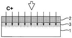
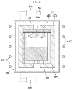
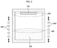
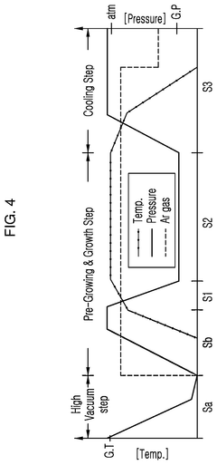
- A method involving the formation of a buffer layer on a silicon substrate, followed by carbon ion implantation and heat treatment in a controlled atmosphere to achieve a single crystal silicon carbide layer with reduced surface roughness without the need for extensive CMP, utilizing adjustments in ion implantation conditions and etching processes to minimize surface defects and enhance crystalline properties.
Silicon carbide wafer and semiconductor device
PatentActiveUS12270122B2
Innovation
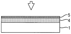
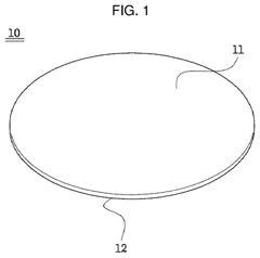
- A silicon carbide wafer with specific surface roughness characteristics, including an average Rmax roughness of 2.0 nm or less and an average Ra roughness of 0.1 nm or less, is developed. The wafer is designed to maintain a uniform quality across its surface, with a controlled difference in roughness between the edge and central regions, and optimized optical properties such as total light transmittance and haze.
Environmental Impact of SiC Processing Methods
The environmental impact of Silicon Carbide (SiC) processing methods represents a critical consideration in the sustainable development of optoelectronic technologies. Traditional SiC wafer manufacturing processes involve energy-intensive operations, including crystal growth at temperatures exceeding 2000°C, which contributes significantly to carbon emissions. The Lely method and physical vapor transport (PVT) techniques, while effective for producing high-quality SiC crystals, consume substantial electrical energy and often utilize graphite components that degrade over time, requiring frequent replacement and generating waste.
Chemical mechanical polishing (CMP), a standard surface engineering technique for SiC wafers, presents additional environmental challenges. The process employs abrasive slurries containing potentially harmful chemicals and nanoparticles that require careful handling and disposal. Wastewater from CMP operations contains suspended solids, heavy metals, and chemical compounds that can contaminate water systems if not properly treated. Furthermore, the significant water consumption during polishing and cleaning stages places pressure on local water resources in manufacturing regions.
Etching processes, particularly reactive ion etching (RIE) and plasma etching, utilize fluorine-based gases such as SF6 and CF4, which are potent greenhouse gases with global warming potentials thousands of times greater than CO2. The semiconductor industry has been working to implement abatement systems to reduce these emissions, but challenges remain in achieving complete mitigation.
Recent advancements in eco-friendly processing methods show promising developments. Dry polishing techniques reduce water consumption and chemical waste, while closed-loop systems for slurry recycling minimize resource depletion. Additionally, manufacturers are exploring alternative crystal growth methods that operate at lower temperatures, such as solution growth techniques, potentially reducing energy requirements by 30-40% compared to conventional methods.
Life cycle assessments of SiC wafer production indicate that the environmental footprint extends beyond manufacturing to include raw material extraction and end-of-life disposal. Silicon carbide itself is chemically stable and non-toxic, but the processing aids and auxiliary materials used in its production can pose environmental risks if not managed properly.
Regulatory frameworks worldwide are increasingly addressing these environmental concerns, with legislation such as the EU's Restriction of Hazardous Substances (RoHS) directive and various clean water acts influencing manufacturing practices. Companies investing in SiC technology for optoelectronics must now balance performance requirements with environmental sustainability, driving innovation in greener processing methods that maintain the exceptional material properties required for advanced applications.
Integration Challenges with Existing Semiconductor Fabrication
The integration of Silicon Carbide (SiC) wafers into existing semiconductor fabrication processes presents significant challenges due to the material's unique properties and requirements. Traditional silicon-based semiconductor manufacturing facilities are not inherently designed to accommodate the higher processing temperatures, different chemical behaviors, and mechanical characteristics of SiC materials.
One primary challenge is the thermal compatibility issue. SiC processing typically requires temperatures exceeding 1600°C, substantially higher than the 1200°C maximum for silicon processing. This necessitates specialized high-temperature furnaces and thermal management systems that many existing fabrication facilities lack. The thermal expansion coefficient mismatch between SiC and conventional materials used in fabrication equipment also creates stress-related complications during thermal cycling.
Surface preparation techniques represent another major integration hurdle. SiC wafers require more aggressive chemical mechanical polishing (CMP) processes due to their exceptional hardness (9.5 on the Mohs scale compared to silicon's 7). Conventional CMP equipment designed for silicon often experiences accelerated wear and reduced efficiency when processing SiC, necessitating significant modifications or replacement.
Contamination control becomes increasingly critical with SiC optoelectronic applications. The material's wide bandgap properties that make it valuable for optoelectronic devices also make it sensitive to certain impurities that might be tolerable in conventional silicon processing. Cross-contamination risks are heightened when facilities attempt to process both silicon and SiC wafers using shared equipment.
Metrology and inspection systems present further integration challenges. Many existing optical inspection tools are calibrated for silicon's optical properties and may not accurately characterize SiC surfaces. The different refractive indices and surface characteristics require recalibration or new equipment investments, adding to integration costs.
Photolithography processes must also be adapted for SiC wafers. The material's different reflectivity and thermal properties affect exposure parameters and resist behavior. Additionally, etching processes for SiC require significantly more aggressive chemistry or plasma conditions than silicon, often necessitating dedicated equipment to prevent damage to tools used for conventional materials.
The economic implications of these integration challenges are substantial. Manufacturers face difficult decisions between creating dedicated SiC processing lines (requiring major capital investment) or attempting partial integration with existing facilities (accepting yield and performance compromises). This integration complexity has contributed to the higher cost structure of SiC-based optoelectronic devices compared to conventional semiconductor alternatives.
Unlock deeper insights with Patsnap Eureka Quick Research — get a full tech report to explore trends and direct your research. Try now!
Generate Your Research Report Instantly with AI Agent
Supercharge your innovation with Patsnap Eureka AI Agent Platform!