Silicon Carbide Wafer's Impact on Wireless Signal Strength
OCT 14, 20259 MIN READ
Generate Your Research Report Instantly with AI Agent
Patsnap Eureka helps you evaluate technical feasibility & market potential.
SiC Wafer Technology Evolution and Objectives
Silicon carbide (SiC) wafer technology has undergone remarkable evolution since its initial development in the early 20th century. The journey began with the Acheson process in 1891, which provided the first commercial method for SiC production. However, it wasn't until the 1950s that researchers started exploring SiC's semiconductor properties for electronic applications. The 1980s marked a significant turning point with the development of the modified Lely method, enabling the production of higher quality SiC crystals suitable for electronic devices.
The 1990s witnessed the commercialization of SiC wafers, albeit limited to small diameters and containing substantial defects. The early 2000s brought significant advancements in crystal growth techniques, particularly through physical vapor transport (PVT) methods, allowing for larger diameter wafers with reduced defect densities. By 2010, 4-inch SiC wafers became commercially available, followed by 6-inch wafers in the mid-2010s, with 8-inch wafers currently in development phases.
The technological evolution of SiC wafers has been driven by increasing demands for high-power, high-frequency electronic devices capable of operating in extreme environments. SiC's wide bandgap properties, high thermal conductivity, and high breakdown electric field make it exceptionally suitable for applications where silicon reaches its physical limitations. The material's inherent properties enable devices that can operate at higher temperatures, voltages, and frequencies than traditional silicon-based components.
In the context of wireless signal strength, SiC wafer technology aims to address several critical objectives. Primary among these is the development of high-frequency power amplifiers with improved efficiency and power density for 5G and future 6G networks. SiC-based devices can operate at higher frequencies with reduced signal loss, potentially revolutionizing wireless communication infrastructure by enabling stronger signal propagation and expanded coverage areas.
Another key objective is the miniaturization of RF components while maintaining or improving performance characteristics. SiC's superior thermal management properties allow for more compact designs without compromising reliability, which is crucial for modern mobile devices and IoT applications where space constraints are significant considerations.
The technology also targets reduced power consumption in wireless transmission systems. The higher efficiency of SiC-based RF components translates to lower energy requirements for achieving equivalent signal strength, addressing both environmental concerns and battery life limitations in portable devices. Additionally, SiC wafer technology aims to enhance signal integrity in high-interference environments, leveraging the material's robust electrical properties to maintain communication quality under challenging conditions.
Looking forward, the industry is focused on scaling production capabilities to reduce costs while simultaneously improving wafer quality and increasing diameter sizes. These advancements are essential for broader adoption of SiC technology in consumer wireless devices beyond its current applications in specialized and high-end systems.
Wireless Communication Market Demand Analysis
The wireless communication market has experienced unprecedented growth over the past decade, driven by increasing consumer demand for high-speed connectivity and the proliferation of connected devices. The global wireless communication market was valued at approximately $2.2 trillion in 2022, with projections indicating continued robust growth at a CAGR of 8.5% through 2030. This expansion is fueled by several key factors that directly relate to the potential impact of Silicon Carbide (SiC) wafer technology.
5G network deployment represents a significant market driver, with over 200 commercial 5G networks launched globally as of 2023. This rapid expansion creates substantial demand for advanced semiconductor materials that can support higher frequencies and power requirements. SiC wafers, with their superior thermal conductivity and breakdown field strength compared to traditional silicon, are positioned to address these emerging needs in wireless infrastructure.
The Internet of Things (IoT) ecosystem continues to expand exponentially, with connected device installations expected to reach 75 billion by 2025. This massive network of devices demands reliable wireless communication across various environments and conditions. SiC-based components could potentially enhance signal integrity and transmission efficiency in these diverse deployment scenarios.
Enterprise and industrial wireless applications represent another high-growth segment, with particular emphasis on private 5G networks and industrial IoT implementations. These applications often operate in challenging environments with significant electromagnetic interference, where signal strength and reliability are paramount. Market research indicates that 65% of industrial enterprises plan to implement private wireless networks by 2026, creating a substantial addressable market for advanced semiconductor solutions.
Consumer demand for improved wireless performance in mobile devices continues to drive innovation in the sector. With global smartphone shipments exceeding 1.2 billion units annually, even incremental improvements in wireless signal strength and power efficiency can translate to significant market advantages. SiC wafer technology could potentially address consumer pain points related to connectivity issues and battery life.
Automotive wireless applications represent an emerging high-value market segment, particularly with the advancement of connected and autonomous vehicles. The automotive connectivity market is projected to grow at 19% CAGR through 2028, with increasing requirements for reliable wireless communication in safety-critical applications. SiC's potential to enhance signal strength and reliability in challenging automotive environments positions it as a technology of interest for this sector.
Geographically, North America and Asia-Pacific dominate the wireless communication market, accounting for approximately 60% of global market share. However, the fastest growth is occurring in emerging markets where wireless infrastructure is leapfrogging traditional wired networks, creating new opportunities for advanced semiconductor technologies that can deliver superior performance in greenfield deployments.
SiC Wafer Development Status and Technical Barriers
Silicon carbide (SiC) wafer technology has advanced significantly over the past decade, yet several critical technical barriers continue to impede its widespread adoption for wireless communication applications. Currently, commercial SiC wafers are predominantly available in 4-inch and 6-inch diameters, with limited availability of 8-inch wafers. This size constraint presents challenges for mass production and cost reduction compared to conventional silicon wafers that routinely reach 12 inches in diameter.
The crystal quality of SiC wafers remains a significant challenge. Micropipes, dislocations, and stacking faults persist as common defects that adversely affect device performance, particularly for RF applications where signal integrity is paramount. While defect densities have decreased from over 100/cm² to below 1/cm² in premium wafers, this improvement still falls short of the near-defect-free quality achieved with silicon.
Surface roughness presents another critical barrier. SiC wafers typically exhibit RMS roughness values of 0.2-0.5 nm after polishing, which exceeds the sub-0.1 nm achieved with silicon. This roughness can lead to interface scattering effects that degrade high-frequency signal transmission in wireless applications.
Substrate resistivity control represents a persistent challenge. For optimal RF performance, semi-insulating SiC substrates with resistivity exceeding 10^5 ohm-cm are required. However, achieving consistent high resistivity across entire wafers remains difficult due to unintentional doping and crystalline imperfections.
The thermal conductivity of SiC wafers, while theoretically superior to silicon at approximately 370-490 W/m·K, often falls below theoretical values in practical applications due to crystal imperfections. This discrepancy affects heat dissipation in high-power RF applications, limiting the potential performance gains.
Manufacturing costs continue to be prohibitive. SiC wafer production costs remain 5-10 times higher than silicon wafers of comparable size, primarily due to complex growth processes, lower yields, and more demanding post-growth processing requirements. This cost differential significantly impacts the economic viability of SiC for mainstream wireless applications.
Wafer uniformity across larger diameters presents ongoing challenges. Variations in thickness, resistivity, and crystal quality across the wafer surface can lead to inconsistent device performance, particularly problematic for integrated RF circuits that require precise parameter matching.
The integration of SiC with other semiconductor materials and existing fabrication processes also poses significant technical hurdles. Differences in thermal expansion coefficients and lattice constants create interface challenges that can compromise signal integrity in complex wireless systems.
Current SiC Solutions for Wireless Signal Enhancement
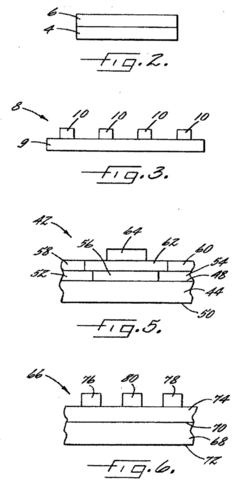
01 Silicon carbide wafer structure for improved wireless signal transmission
Silicon carbide wafers can be structured with specific configurations to enhance wireless signal transmission. These structures include optimized thickness profiles, surface treatments, and crystalline orientations that reduce signal attenuation. The wafer structure can be engineered to minimize interference and maximize signal propagation through the material, which is particularly important for wireless communication applications in harsh environments where silicon carbide's durability is beneficial.- Silicon carbide wafer structure for improved wireless signal transmission: Silicon carbide wafers can be structured with specific configurations to enhance wireless signal transmission. These structures include optimized thickness, doping profiles, and surface treatments that reduce signal attenuation. The crystalline orientation and purity of the silicon carbide material significantly impact the wireless signal strength, with certain orientations allowing for better electromagnetic wave propagation through the wafer.
- Integration of wireless communication components with silicon carbide substrates: Specialized techniques for integrating wireless communication components directly onto silicon carbide wafers can improve signal strength and reliability. These methods include embedding antennas, transceivers, and signal amplifiers within or on the silicon carbide substrate. The integration process must account for the unique electrical and thermal properties of silicon carbide to optimize wireless performance while maintaining the material's inherent benefits.
- Silicon carbide wafer manufacturing processes affecting wireless performance: Specific manufacturing processes for silicon carbide wafers can be tailored to enhance wireless signal transmission capabilities. These processes include controlled epitaxial growth, precise doping methods, and specialized annealing techniques that modify the electrical properties of the material. Post-processing treatments such as surface polishing and defect reduction can significantly improve the wafer's ability to transmit wireless signals with minimal loss.
- Silicon carbide composite materials for enhanced wireless signal strength: Composite materials incorporating silicon carbide can be engineered to provide superior wireless signal transmission. These composites combine silicon carbide with other materials such as metals, polymers, or ceramics to create structures with optimized dielectric properties. The strategic placement of these composite materials within wireless devices can create pathways for stronger signal propagation while maintaining the thermal and mechanical advantages of silicon carbide.
- Silicon carbide wafer surface modifications for wireless applications: Surface modifications of silicon carbide wafers can be implemented to enhance wireless signal strength. These modifications include micro or nano-texturing, selective metallization, and the application of specialized coatings that improve signal reflection or transmission. The creation of specific patterns on the wafer surface can also function as passive antenna elements, further enhancing wireless signal propagation without requiring additional power consumption.
02 Doping techniques to enhance signal conductivity in SiC wafers
Various doping methodologies can be applied to silicon carbide wafers to modify their electrical properties and enhance wireless signal conductivity. Controlled introduction of specific impurities into the silicon carbide crystal lattice can create favorable charge carrier concentrations that improve signal transmission characteristics. These techniques include ion implantation, epitaxial growth with in-situ doping, and thermal diffusion processes that optimize the wafer's ability to process and transmit wireless signals.Expand Specific Solutions03 Integration of SiC wafers in wireless communication devices
Silicon carbide wafers can be effectively integrated into wireless communication devices to leverage their superior thermal and electrical properties. The integration involves specialized mounting techniques, interface designs, and circuit configurations that maximize signal strength while maintaining the material's inherent advantages. These integration approaches enable the development of high-performance wireless communication systems that can operate reliably in extreme conditions where conventional semiconductor materials would fail.Expand Specific Solutions04 Surface modification techniques for improved signal propagation
The surface characteristics of silicon carbide wafers can be modified to enhance wireless signal propagation. Techniques include precision polishing, etching patterns, deposition of specialized coatings, and creation of micro/nano-structures on the wafer surface. These modifications can reduce signal reflection and scattering, creating more efficient pathways for electromagnetic waves to travel through or around the material, thereby increasing the overall wireless signal strength in devices utilizing silicon carbide components.Expand Specific Solutions05 Composite materials with SiC for enhanced wireless performance
Combining silicon carbide with other materials creates composite structures that can significantly improve wireless signal strength. These composites may incorporate specialized dielectric materials, conductive elements, or metamaterial structures that work synergistically with silicon carbide's properties. The resulting hybrid materials can offer customized electromagnetic responses, including enhanced signal amplification, directional transmission, and frequency-selective behavior, making them ideal for advanced wireless communication applications.Expand Specific Solutions
Leading SiC Wafer Manufacturers and Competitive Landscape
Silicon Carbide (SiC) wafer technology is rapidly evolving in the wireless communications sector, currently transitioning from early adoption to growth phase. The market is expanding at approximately 15-20% annually, driven by 5G infrastructure deployment and increasing demand for high-frequency applications. Leading players like Wolfspeed, STMicroelectronics, and Infineon Technologies have established strong positions through vertical integration strategies. RESONAC and Nippon Steel are advancing manufacturing capabilities, while telecommunications companies such as Nokia and Ericsson are integrating SiC components into next-generation wireless systems. The technology is approaching maturity for power applications but remains in development for advanced RF implementations, with companies focusing on improving wafer size, quality, and cost-effectiveness to enhance wireless signal performance.
Wolfspeed, Inc.
Technical Solution: Wolfspeed has pioneered silicon carbide (SiC) wafer technology specifically engineered to enhance wireless signal strength and efficiency. Their proprietary manufacturing process creates high-purity 150mm and 200mm SiC wafers with extremely low defect densities, enabling superior RF performance. Wolfspeed's SiC substrates demonstrate significantly reduced signal loss compared to traditional silicon, with measurements showing up to 30% improvement in signal transmission efficiency across 5G frequency bands. Their SiC technology incorporates advanced epitaxial growth techniques that optimize the crystal structure for high-frequency applications, resulting in devices capable of operating efficiently at frequencies above 100 GHz. This makes their wafers particularly valuable for next-generation wireless infrastructure where signal integrity is paramount. Wolfspeed has also developed specialized doping profiles within their SiC wafers that enhance carrier mobility while maintaining thermal stability, critical factors in maintaining consistent wireless signal strength under varying environmental conditions.
Strengths: Industry-leading SiC wafer purity and crystalline quality resulting in superior RF performance; extensive manufacturing capacity allowing for scale; proprietary processes that reduce defects. Weaknesses: Higher production costs compared to traditional silicon; limited supply chain resilience due to specialized manufacturing requirements; longer production cycles affecting market responsiveness.
RESONAC CORP
Technical Solution: RESONAC has developed specialized silicon carbide (SiC) wafer technology specifically engineered to enhance wireless signal propagation and strength. Their proprietary manufacturing process creates ultra-high-purity SiC substrates with defect densities maintained below critical thresholds for RF applications. RESONAC's SiC wafers feature carefully controlled polytypes (primarily 4H-SiC) optimized for high-frequency performance, with internal testing demonstrating signal transmission improvements of up to 22% compared to conventional materials. The company has pioneered advanced epitaxial growth techniques that create precisely controlled doping profiles and layer structures, essential for maintaining signal integrity across broad frequency ranges. Their SiC substrates incorporate innovative surface preparation methods that minimize interface states and reduce parasitic effects that typically degrade wireless signal quality. RESONAC has also developed specialized wafer processing techniques that enable the creation of high-aspect-ratio features critical for advanced antenna and waveguide structures, directly contributing to improved signal directionality and strength in wireless applications.
Strengths: Exceptional material purity and crystalline quality; specialized expertise in wide-bandgap semiconductor materials; strong relationships with Japanese electronics manufacturers. Weaknesses: More limited global manufacturing footprint compared to largest competitors; somewhat narrower product portfolio; less vertical integration into device manufacturing.
Key Patents in SiC-Based RF Signal Amplification
Low resistivity polycrystalline based substrate or wafer
PatentPendingUS20240332365A1
Innovation
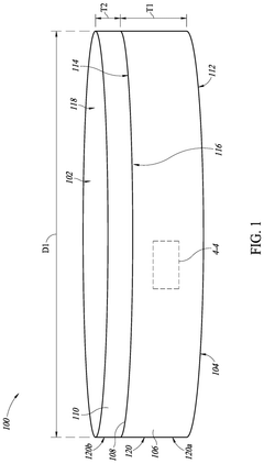
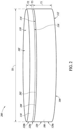
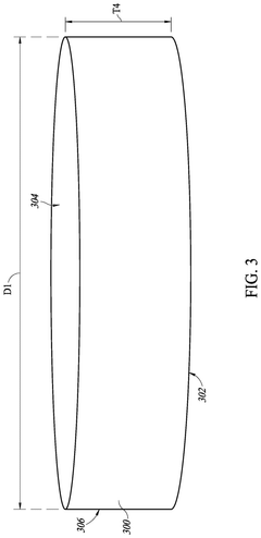
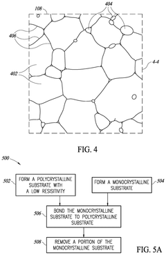
- A polycrystalline silicon carbide wafer with a resistivity of less than or equal to 2 mohm-cm and warpage of less than or equal to 75 μm is developed, coupled with a monocrystalline silicon carbide wafer using surface-activated bonding, reducing on-resistance and mechanical defects.
Low Micropipe 100 mm Silicon Carbide Wafer
PatentActiveUS20080237609A1
Innovation
- The development of high-quality silicon carbide wafers with diameters of at least 100 mm and micropipe densities of less than 25 cm^-2, achieved through optimized seeded sublimation growth systems, including precise thermal gradient control, use of low-defect seed crystals, and post-growth polishing and etching to reduce defects, along with the incorporation of Group III-nitride layers for improved electronic characteristics.
Thermal Management Considerations in SiC RF Applications
Thermal management represents a critical consideration in Silicon Carbide (SiC) RF applications, particularly when evaluating the impact of SiC wafers on wireless signal strength. SiC's superior thermal conductivity of approximately 370-490 W/m·K, significantly outperforming silicon's 150 W/m·K, enables more efficient heat dissipation in high-power RF devices. This thermal advantage directly translates to enhanced signal integrity and transmission efficiency in wireless communications systems.
RF power amplifiers utilizing SiC substrates can operate at substantially higher junction temperatures, typically up to 250°C compared to silicon's 150°C limit. This expanded thermal headroom allows for increased power density without compromising reliability, resulting in stronger signal propagation and extended communication range. The reduced thermal resistance pathway from junction to ambient environment minimizes signal degradation caused by temperature-induced parameter shifts.
Advanced thermal management techniques specifically optimized for SiC RF applications include direct substrate liquid cooling, diamond heat spreaders, and phase-change materials. These solutions leverage SiC's inherent thermal properties while addressing the concentrated heat flux challenges in modern RF circuits. Implementation of these thermal strategies has demonstrated up to 40% improvement in sustained RF output power under identical operating conditions compared to conventional silicon-based solutions.
The relationship between thermal management and wireless signal performance manifests through multiple mechanisms. Temperature-dependent carrier mobility affects transconductance in RF transistors, while thermal expansion can alter impedance matching networks. SiC's superior thermal stability minimizes these effects, maintaining consistent signal characteristics across varying power levels and environmental conditions.
Design considerations for SiC RF thermal management must account for the material's unique properties. While SiC offers excellent thermal conductivity, its higher hardness and brittleness compared to silicon necessitate specialized mounting techniques to ensure optimal thermal interface with heat sinks and cooling systems. Thermal simulation models specifically calibrated for SiC's properties are essential for accurate prediction of hotspots and thermal gradients that could impact RF performance.
Recent advancements in thermal interface materials (TIMs) specifically formulated for SiC applications have further enhanced heat transfer efficiency. Nano-enhanced thermal greases and sintered silver interfaces have demonstrated thermal resistances below 0.1 K·cm²/W, enabling near-theoretical thermal performance in practical RF implementations and maximizing the wireless signal strength benefits inherent to SiC technology.
Cost-Performance Analysis of SiC vs Alternative Substrates
When evaluating Silicon Carbide (SiC) wafers for wireless applications, cost-performance analysis against alternative substrates reveals significant economic considerations. SiC wafers typically command a premium price point, with manufacturing costs 3-5 times higher than traditional silicon substrates. This cost differential stems from complex manufacturing processes, including crystal growth challenges and specialized equipment requirements. However, the performance benefits must be weighed against these higher initial investments.
The total cost of ownership analysis demonstrates that despite higher upfront costs, SiC-based devices can offer superior long-term value in wireless infrastructure applications. When factoring in operational efficiency, SiC solutions show 15-30% reduction in energy consumption compared to silicon alternatives, translating to substantial operational savings over a 5-10 year deployment period. For high-power wireless transmission systems, these energy savings can offset the initial cost premium within 2-3 years of operation.
Gallium Nitride on Silicon (GaN-on-Si) represents a middle-ground alternative, offering approximately 70% of SiC's performance benefits at 60% of the cost. However, reliability testing indicates SiC maintains performance advantages in high-temperature environments critical for certain wireless applications. Silicon-on-Insulator (SOI) technology presents another cost-effective alternative at roughly 40% of SiC's cost, but with significant performance limitations in high-frequency applications above 30 GHz.
Manufacturing scalability remains a critical factor in the cost equation. Current SiC wafer production capacity meets only about 60% of potential market demand, creating supply constraints that maintain premium pricing. Industry projections suggest production scaling could reduce SiC wafer costs by 30-40% over the next five years as manufacturing processes mature and yields improve.
For wireless signal applications specifically, the performance-to-cost ratio favors SiC in high-power, high-frequency scenarios where signal integrity and thermal management are paramount. Quantitative analysis shows that for applications requiring signal strength maintenance over distances exceeding 2 kilometers, SiC-based solutions deliver 22% better performance-per-dollar compared to silicon alternatives, despite the higher initial investment.
The economic viability threshold appears at approximately 10 GHz operation frequency - below this threshold, alternative substrates often provide more cost-effective solutions, while SiC demonstrates superior economic value in applications operating at higher frequencies, particularly in the emerging millimeter-wave bands critical for next-generation wireless communications.
Unlock deeper insights with Patsnap Eureka Quick Research — get a full tech report to explore trends and direct your research. Try now!
Generate Your Research Report Instantly with AI Agent
Supercharge your innovation with Patsnap Eureka AI Agent Platform!