Silicon Carbide Wafer Adoption in Next-Generation Radar Technology
OCT 14, 20259 MIN READ
Generate Your Research Report Instantly with AI Agent
Patsnap Eureka helps you evaluate technical feasibility & market potential.
SiC Wafer Evolution and Radar Integration Goals
Silicon Carbide (SiC) wafer technology has undergone significant evolution since its initial development in the early 1990s. The journey began with small-diameter wafers plagued by high defect densities and limited production capabilities. Early SiC wafers were primarily 2-inch in diameter with micropipe densities exceeding 100 per cm², severely limiting their application potential. The technological progression has been remarkable, with current commercial offerings including 6-inch and emerging 8-inch wafers featuring defect densities below 1 per cm², representing a hundredfold improvement in quality.
This evolution has been driven by innovations in crystal growth techniques, transitioning from the primitive modified Lely method to advanced physical vapor transport (PVT) processes. Significant breakthroughs in seeding technology and thermal gradient control have enabled larger diameter wafers with superior crystalline quality. The development of advanced polishing techniques has also contributed to achieving atomically smooth surfaces essential for device fabrication.
The integration of SiC wafers into radar technology represents a paradigm shift in performance capabilities. Traditional radar systems based on silicon or gallium arsenide semiconductors face fundamental limitations in power handling, operating frequency, and thermal management. SiC-based devices offer breakthrough potential with their wide bandgap (3.26 eV), high breakdown field strength (2.8 MV/cm), and superior thermal conductivity (3.7 W/cm·K).
The primary goal of SiC wafer adoption in next-generation radar technology is to enable high-power, high-frequency operation in extreme environments. Military and aerospace applications demand radar systems capable of functioning reliably at temperatures exceeding 200°C while maintaining signal integrity. SiC-based power amplifiers and transmit/receive modules can potentially operate at junction temperatures 100°C higher than conventional technologies, dramatically improving reliability in harsh conditions.
Another critical objective is the development of more compact radar systems with enhanced detection capabilities. The higher power density of SiC allows for significant miniaturization while maintaining or improving performance metrics. This is particularly valuable for airborne and space-based radar platforms where size and weight constraints are paramount. The target is to achieve a 40% reduction in system volume while extending detection range by 30%.
Energy efficiency represents another key goal, with SiC-based radar systems aiming to reduce power consumption by 25-35% compared to conventional technologies. This efficiency improvement stems from higher operating frequencies, reduced switching losses, and better thermal management, collectively enabling more sustainable operation and extended mission durations for autonomous platforms.
Market Analysis for SiC-Based Radar Systems
The global market for Silicon Carbide (SiC) based radar systems is experiencing unprecedented growth, driven primarily by advancements in automotive, defense, and aerospace sectors. Current market valuations indicate that the SiC power semiconductor market reached approximately $1.5 billion in 2022, with radar applications constituting a significant portion of this value. Industry analysts project a compound annual growth rate (CAGR) of 18-20% for SiC-based radar systems through 2030, substantially outpacing traditional silicon-based alternatives.
The automotive sector represents the largest market segment for SiC radar systems, accounting for nearly 45% of the total market share. This dominance stems from the increasing integration of advanced driver assistance systems (ADAS) and autonomous driving capabilities in modern vehicles. Premium automotive manufacturers have already begun incorporating SiC-based radar systems in their high-end models, with mass-market adoption expected to accelerate between 2025-2027.
Defense applications constitute the second-largest market segment at approximately 30% market share. Military radar systems benefit significantly from SiC's superior performance in high-power, high-frequency operations. Major defense contractors in North America and Europe have allocated substantial R&D budgets toward SiC radar technology, with procurement cycles expected to mature within the next 3-5 years.
Regional analysis reveals North America currently leads the market with 38% share, followed by Europe (29%) and Asia-Pacific (26%). However, the Asia-Pacific region is projected to witness the fastest growth rate, driven by China's ambitious investments in both automotive and defense sectors, alongside Japan's strong position in automotive radar technology.
Key market drivers include the increasing demand for higher resolution and longer-range radar systems, particularly for autonomous vehicles and advanced military applications. The superior thermal conductivity and breakdown field strength of SiC wafers enable radar systems to operate at higher power densities and frequencies, delivering enhanced performance in adverse environmental conditions.
Market barriers primarily revolve around cost considerations, with SiC wafers currently commanding a premium of 3-4 times that of traditional silicon alternatives. However, economies of scale and manufacturing improvements are gradually reducing this cost differential, with price parity for certain applications expected by 2028-2030.
Customer segmentation analysis indicates that tier-one automotive suppliers and prime defense contractors represent the primary customer base, with emerging opportunities in commercial aerospace and industrial automation sectors. The market exhibits moderate concentration, with the top five suppliers controlling approximately 65% of the global market share.
SiC Wafer Technology Status and Challenges
Silicon Carbide (SiC) wafer technology has reached a critical juncture in its development trajectory, with significant advancements enabling its potential adoption in next-generation radar systems. Currently, SiC wafers are predominantly available in 4-inch and 6-inch diameters, with leading manufacturers beginning limited production of 8-inch wafers. This represents substantial progress from the early 2000s when only 2-inch wafers were commercially viable, though still lags behind silicon technology which routinely produces 12-inch wafers.
The primary technical challenge facing SiC wafer production remains the difficulty in growing high-quality single crystals with minimal defects. Micropipe defects, though significantly reduced in recent years to below 1 cm^-2 in premium wafers, continue to impact device yield and reliability. Basal plane dislocations and stacking faults represent additional defect categories that compromise wafer quality and performance in high-power applications typical of radar systems.
Material purity presents another significant hurdle, as trace impurities can dramatically alter the electrical properties of SiC devices. Current production methods struggle to consistently achieve the ultra-high purity levels required for advanced radar applications, particularly in terms of controlling nitrogen and aluminum dopant concentrations with precision across the entire wafer surface.
Manufacturing costs remain prohibitively high compared to silicon alternatives, with SiC wafers typically costing 5-10 times more than silicon wafers of comparable size. This cost differential stems from complex growth processes, lower yields, and the extreme processing conditions required for SiC crystal growth, including temperatures exceeding 2000°C and precisely controlled pressure environments.
Geographically, SiC wafer production capability is concentrated in a limited number of regions. The United States, Japan, and Germany lead in high-quality SiC wafer manufacturing, with China rapidly expanding its production capacity. This concentration creates potential supply chain vulnerabilities for radar technology developers seeking to incorporate SiC components.
Surface finishing quality represents another technical challenge, as SiC's extreme hardness (second only to diamond) makes achieving the ultra-smooth surfaces required for complex device fabrication difficult. Current chemical-mechanical polishing techniques struggle to consistently deliver the sub-nanometer surface roughness ideal for advanced radar applications.
The integration of SiC wafers into existing semiconductor fabrication lines presents compatibility challenges, as many processes optimized for silicon require significant modification to accommodate SiC's different thermal, chemical, and mechanical properties. This necessitates specialized equipment and process development, further increasing the barriers to widespread adoption in radar applications.
Current SiC Implementation in Radar Applications
01 Silicon Carbide Wafer Manufacturing Methods
Various manufacturing methods are employed to produce high-quality silicon carbide wafers for semiconductor applications. These methods include chemical vapor deposition (CVD), physical vapor transport (PVT), and modified Lely processes. The manufacturing techniques focus on controlling crystal growth, reducing defects, and achieving specific polytype formations such as 4H-SiC or 6H-SiC. Advanced processes have been developed to increase wafer diameter while maintaining structural integrity and electrical properties.- Silicon Carbide Wafer Manufacturing Methods: Various manufacturing methods are employed to produce high-quality silicon carbide wafers, including chemical vapor deposition (CVD), physical vapor transport (PVT), and modified Lely methods. These processes focus on controlling crystal growth conditions to minimize defects and achieve desired wafer properties. Advanced techniques have been developed to grow large-diameter SiC single crystals with improved uniformity and reduced micropipe density.
- Defect Reduction Techniques in SiC Wafers: Techniques for reducing defects in silicon carbide wafers include specialized annealing processes, surface treatment methods, and defect conversion mechanisms. These approaches target common SiC defect types such as basal plane dislocations, micropipes, and stacking faults. Advanced characterization and processing methods help identify and eliminate defects to improve wafer quality and device performance.
- SiC Wafer Surface Processing and Preparation: Surface processing techniques for silicon carbide wafers include chemical-mechanical polishing (CMP), plasma etching, and specialized cleaning methods. These processes aim to achieve atomically smooth surfaces with minimal subsurface damage, which is critical for subsequent epitaxial growth and device fabrication. Advanced surface preparation methods help improve interface quality and reduce surface-related defects.
- Epitaxial Growth on SiC Wafers: Epitaxial layer growth on silicon carbide wafers involves controlled deposition of thin films with specific doping profiles and thickness uniformity. Various epitaxial growth techniques are employed, including chemical vapor deposition (CVD) with specialized precursors and growth conditions. These epitaxial layers form the active regions for high-power and high-frequency electronic devices, with methods focused on achieving high crystal quality and precise doping control.
- SiC Wafer Applications in Power Electronics: Silicon carbide wafers are increasingly used in power electronics applications due to their superior properties compared to silicon, including higher breakdown voltage, thermal conductivity, and switching speed. SiC-based devices such as MOSFETs, Schottky diodes, and JFETs enable more efficient power conversion systems with higher operating temperatures and frequencies. These advantages make SiC wafers particularly valuable for electric vehicles, renewable energy systems, and industrial power applications.
02 Defect Reduction Techniques in SiC Wafers
Techniques for reducing defects in silicon carbide wafers are critical for improving semiconductor device performance. These include thermal annealing processes, surface polishing methods, and specialized etching techniques to eliminate micropipes, dislocations, and stacking faults. Advanced characterization methods help identify and mitigate basal plane dislocations and other crystallographic defects that can affect device reliability. These techniques collectively enhance the structural quality and electrical performance of SiC wafers.Expand Specific Solutions03 SiC Wafer Surface Treatment and Preparation
Surface treatment and preparation processes for silicon carbide wafers include chemical-mechanical polishing (CMP), plasma etching, and thermal oxidation. These processes aim to achieve atomically smooth surfaces with minimal subsurface damage, which is essential for subsequent epitaxial growth and device fabrication. Various cleaning protocols remove contaminants and create specific surface terminations to enhance device performance. Advanced surface engineering techniques modify the wafer surface properties to improve electrical characteristics and interface quality.Expand Specific Solutions04 Epitaxial Growth on SiC Wafers
Epitaxial layer growth on silicon carbide wafers involves controlled deposition of thin films with specific doping profiles and thickness uniformity. Techniques such as chemical vapor deposition (CVD) and molecular beam epitaxy (MBE) are used to grow high-quality epitaxial layers for power devices and RF applications. Process parameters including temperature, pressure, and gas flow rates are optimized to achieve desired electrical properties and minimize defect propagation from the substrate. Multi-layer epitaxial structures enable advanced device architectures with enhanced performance characteristics.Expand Specific Solutions05 SiC Wafer Applications in Power Electronics
Silicon carbide wafers are increasingly used in power electronic applications due to their wide bandgap properties, high thermal conductivity, and high breakdown field strength. These characteristics enable the development of high-voltage, high-temperature, and high-frequency devices such as MOSFETs, Schottky diodes, and JFETs. SiC-based power devices offer significant advantages over silicon counterparts, including reduced switching losses, higher efficiency, and smaller form factors. Applications span electric vehicles, renewable energy systems, industrial drives, and high-reliability aerospace electronics.Expand Specific Solutions
Leading SiC Wafer and Radar Technology Companies
The Silicon Carbide (SiC) wafer market for next-generation radar technology is in a growth phase, with increasing adoption driven by SiC's superior performance in high-power, high-frequency applications. The market is expanding rapidly, projected to reach significant scale as radar systems evolve for defense, automotive, and aerospace applications. Leading players demonstrate varying levels of technological maturity: Wolfspeed stands as the dominant force in SiC wafer production, while companies like RESONAC, Siltronic, and NIPPON STEEL are advancing manufacturing capabilities. Newer entrants such as Hunan Sanan and Tongwei Microelectronics are accelerating innovation, particularly in China. Infineon and Advantest represent the application side, integrating SiC into advanced radar systems. The competitive landscape is characterized by strategic partnerships between wafer manufacturers and radar technology developers to overcome production challenges and meet growing demand.
Wolfspeed, Inc.
Technical Solution: Wolfspeed has pioneered the development of silicon carbide (SiC) wafers specifically optimized for radar applications, featuring 150mm and 200mm diameter options with extremely low micropipe density (<1 cm²). Their proprietary high-purity SiC substrate manufacturing process enables the production of wafers with superior thermal conductivity (>350 W/mK) and breakdown field strength (2.8 MV/cm), critical for next-generation radar systems operating at higher frequencies (X-band and beyond). Wolfspeed's vertical integration approach encompasses substrate growth, epitaxial layer deposition, and device fabrication, allowing for tight quality control throughout the production chain. Their SiC wafers demonstrate exceptional uniformity with thickness variation <±10μm and resistivity variation <±15%, enabling the fabrication of high-performance GaN-on-SiC HEMT structures that deliver 5-7dB higher output power compared to traditional GaAs solutions for radar applications.
Strengths: Industry-leading SiC substrate quality with lowest defect density; complete vertical integration from material to device; proven reliability in defense and aerospace applications. Weaknesses: Higher cost compared to silicon alternatives; limited production capacity relative to growing demand; longer lead times for specialized radar-grade wafers.
RESONAC CORP
Technical Solution: RESONAC (formerly Showa Denko) has developed advanced SiC epitaxial wafer technology specifically optimized for radar applications, featuring their proprietary high-temperature CVD process. Their SiC wafers are available in both 4H and 6H polytypes with diameters up to 150mm, featuring extremely low basal plane dislocation densities (<1×10³ cm⁻²) and micropipe densities approaching zero defects per wafer. For radar applications, RESONAC has engineered specialized n-type and semi-insulating SiC substrates with controlled resistivity ranges (0.015-0.028 Ω·cm for n-type and >10⁵ Ω·cm for semi-insulating), enabling optimal performance across different radar subsystems. Their epitaxial growth technology achieves thickness uniformity within ±3% across the wafer, critical for maintaining consistent device performance in phased array radar systems. RESONAC's SiC wafers incorporate proprietary edge treatment processes that reduce edge-related defects by over 80% compared to standard processing, significantly improving device yield for radar MMICs. Their materials have demonstrated excellent high-frequency performance, supporting power densities exceeding 4.5W/mm at X-band frequencies with minimal performance degradation at elevated temperatures.
Strengths: Exceptional material quality with near-zero micropipe density; specialized expertise in epitaxial growth processes; established supplier to defense and aerospace industries. Weaknesses: More limited global presence compared to some competitors; smaller production capacity; less vertical integration into device manufacturing.
Critical Patents in SiC Wafer Manufacturing
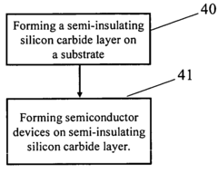
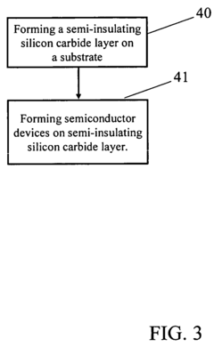
Silicon carbide and related wide-bandgap transistors on semi-insulating epitaxy for high-speed, high-power applications
PatentInactiveUS7432171B2
Innovation
- A semi-insulating (SI) epitaxy layer is used over a conducting wide bandgap substrate, allowing for the use of low-cost, high-quality n-type substrates while maintaining the benefits of semi-insulating material, which reduces defect density and enhances device reliability by isolating active areas and improving thermal conductivity.
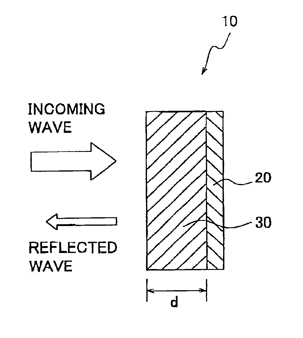
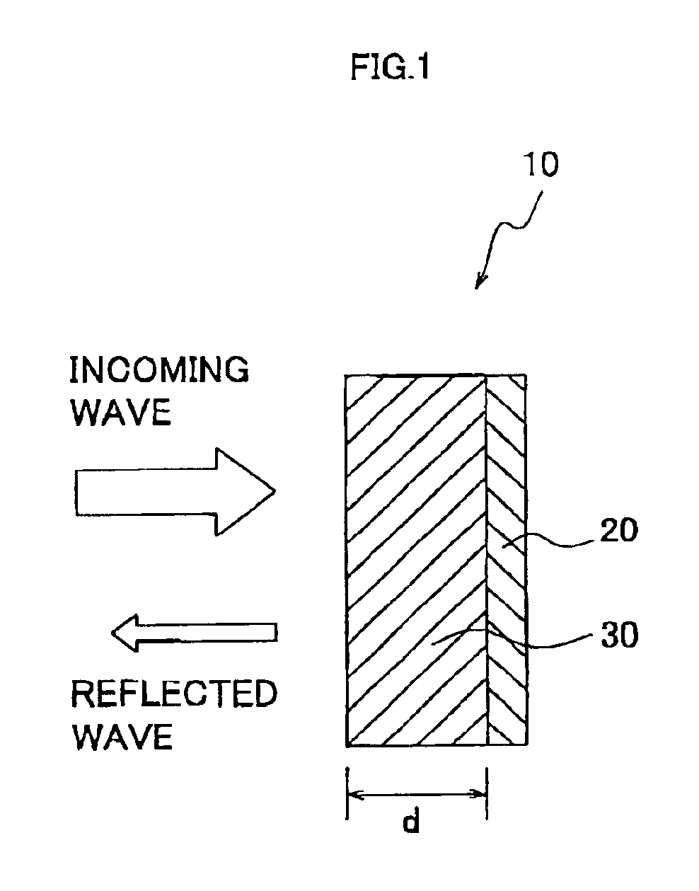
Radio wave absorber and production method thereof
PatentInactiveUS6870497B2
Innovation
- A laminated radio wave absorber with a radio wave absorbing layer made from silicon carbide powder dispersed in matrix resin, where the average particle diameter of the powder is 4-40 μm and the content is 15-45 volume %, providing a thickness for reflection attenuation of not less than 10 dB in the 75-77 GHz frequency band, utilizing ethylene-propylene rubber as the matrix resin and an integrally-molded structure with an adhesive layer.
Thermal Management Solutions for SiC Radar Systems
The thermal management of Silicon Carbide (SiC) radar systems presents unique challenges due to the high power density and operating temperatures of SiC devices. As radar systems evolve to incorporate SiC wafer technology, traditional cooling methods become insufficient to handle the increased thermal loads. Effective thermal management is critical to ensure system reliability, performance, and longevity in next-generation radar applications.
SiC-based radar systems typically generate heat fluxes exceeding 500 W/cm², significantly higher than traditional silicon-based systems. This necessitates advanced cooling solutions that can efficiently dissipate heat while maintaining junction temperatures below 175°C for optimal performance. The thermal conductivity advantage of SiC (approximately 3-4 times that of silicon) provides some inherent benefits, but system-level thermal management remains essential.
Current thermal management approaches for SiC radar systems include advanced liquid cooling technologies, such as microchannel cold plates and direct liquid impingement. These solutions achieve thermal resistances as low as 0.1°C/W and can handle heat fluxes up to 1000 W/cm². Implementation typically involves integrating these cooling structures directly with SiC power amplifiers and transmit/receive modules to minimize thermal resistance paths.
Phase change materials (PCMs) represent another promising solution, particularly for pulsed radar applications. PCMs can absorb large amounts of heat during high-power transmission phases and release it during lower-power reception phases, effectively smoothing thermal transients. Recent developments in metal-embedded PCMs have demonstrated thermal capacities of 200-300 J/cm³, making them suitable for high-power SiC radar applications.
Advanced thermal interface materials (TIMs) are critical components in the thermal management stack. Diamond-filled composites and liquid metal TIMs have shown thermal conductivities exceeding 20 W/m·K, significantly reducing interface thermal resistance between SiC devices and cooling solutions. These materials are particularly important for maintaining thermal performance over thousands of thermal cycles in radar applications.
Computational fluid dynamics (CFD) modeling has become essential for optimizing thermal management solutions for SiC radar systems. Multi-physics simulations that couple electromagnetic, thermal, and mechanical analyses enable accurate prediction of hotspots and thermal gradients. These tools have reduced design iteration cycles by approximately 40% and improved thermal solution effectiveness by 25-30% in recent SiC radar developments.
The integration of thermal management with radar system packaging presents additional challenges. 3D heterogeneous integration approaches that incorporate thermal vias, embedded heat spreaders, and conformal cooling channels have demonstrated promising results. These integrated solutions have achieved up to 50% reduction in thermal resistance compared to conventional approaches while maintaining radar performance parameters.
Military and Aerospace Compliance Requirements
The adoption of Silicon Carbide (SiC) wafers in next-generation radar technology for military and aerospace applications necessitates strict adherence to rigorous compliance requirements. These requirements ensure that radar systems operate reliably in extreme conditions while meeting security and performance standards essential for defense and aerospace operations.
MIL-STD-883 serves as a cornerstone for testing microelectronic devices in military applications, with SiC-based radar components requiring certification under these protocols. The standard encompasses environmental, mechanical, and electrical testing methodologies that verify operational integrity under extreme temperature variations, high-altitude conditions, and intense vibration scenarios commonly encountered in aerospace environments.
DO-254 compliance represents another critical requirement for hardware components in airborne systems. SiC wafer-based radar modules must demonstrate design assurance levels appropriate for their safety-critical functions. This certification process involves comprehensive documentation of design processes, verification methods, and validation procedures to ensure consistent performance throughout the product lifecycle.
Radiation hardening requirements present unique challenges for SiC implementation in space-based radar systems. While SiC inherently offers superior radiation resistance compared to silicon, manufacturers must still meet specific Total Ionizing Dose (TID) thresholds defined by NASA and ESA standards. Qualification testing typically involves exposure to gamma radiation sources to verify continued functionality in the harsh radiation environment of space.
Supply chain security compliance has gained prominence in recent years, with DFARS 252.246-7007 and NIST SP 800-161 establishing frameworks for counterfeit prevention and secure sourcing. For SiC wafers, this translates to stringent traceability requirements from raw material to finished component, with documentation of all processing steps and handling procedures.
Electromagnetic compatibility standards, including MIL-STD-461, govern the electromagnetic emission and susceptibility characteristics of radar systems. SiC-based power amplifiers in radar applications must demonstrate compliance with conducted and radiated emission limits while maintaining immunity to external electromagnetic interference that could compromise system performance.
Export control regulations, particularly ITAR and EAR restrictions, significantly impact the international development and deployment of SiC radar technology. These controls limit the sharing of technical data and physical components with foreign entities, requiring manufacturers to implement robust compliance programs that track and control access to controlled technical information.
Unlock deeper insights with Patsnap Eureka Quick Research — get a full tech report to explore trends and direct your research. Try now!
Generate Your Research Report Instantly with AI Agent
Supercharge your innovation with Patsnap Eureka AI Agent Platform!