Understanding Market Trends for Spintronic Device Applications
OCT 21, 20259 MIN READ
Generate Your Research Report Instantly with AI Agent
Patsnap Eureka helps you evaluate technical feasibility & market potential.
Spintronics Evolution and Research Objectives
Spintronics has evolved significantly since the discovery of giant magnetoresistance (GMR) in the late 1980s by Albert Fert and Peter Grünberg, who were awarded the Nobel Prize in Physics in 2007 for this breakthrough. This discovery marked the beginning of a new era in electronics, where both the charge and spin properties of electrons could be exploited for information processing and storage. The field has since progressed through several key phases, including the development of tunnel magnetoresistance (TMR), spin-transfer torque (STT), and more recently, spin-orbit torque (SOT) technologies.
The evolution of spintronics has been driven by the increasing demands for higher storage density, faster processing speeds, and lower power consumption in electronic devices. Traditional semiconductor-based electronics are approaching their physical limits in terms of miniaturization and energy efficiency, creating an urgent need for alternative technologies. Spintronics offers promising solutions to these challenges by utilizing the spin degree of freedom of electrons, which can be manipulated with minimal energy dissipation.
Current research in spintronics is focused on several key objectives. First, there is a strong emphasis on developing materials with enhanced spin-dependent properties, such as high spin polarization, long spin coherence times, and efficient spin injection capabilities. This includes research into ferromagnetic metals, half-metals, magnetic semiconductors, and topological insulators. Second, researchers are working on improving the efficiency of spin-to-charge conversion mechanisms, which are crucial for reading and writing spin information.
Another important research objective is the integration of spintronic devices with conventional CMOS technology to create hybrid systems that leverage the advantages of both approaches. This includes the development of spin-based logic devices, non-volatile magnetic random-access memory (MRAM), and spin-based sensors. The goal is to create a seamless interface between spin-based and charge-based components, enabling new functionalities while maintaining compatibility with existing infrastructure.
Looking forward, the field is moving towards more complex spintronic systems that exploit quantum effects for information processing. This includes research into quantum spintronics, where quantum coherence and entanglement of spin states could enable quantum computing and quantum communication applications. Additionally, there is growing interest in neuromorphic computing architectures based on spintronic devices, which could mimic the brain's energy-efficient information processing capabilities.
The ultimate objective of spintronic research is to develop commercially viable devices that offer significant advantages over conventional electronics in terms of performance, energy efficiency, and functionality. This requires addressing challenges related to materials science, device physics, fabrication techniques, and system-level integration, necessitating a multidisciplinary approach that combines expertise from physics, materials science, electrical engineering, and computer science.
Market Analysis for Spintronic Applications
The global market for spintronic devices is experiencing significant growth, driven by increasing demand for high-performance computing, data storage solutions, and advanced sensing applications. Current market valuations place the spintronic technology sector at approximately 12.5 billion USD in 2023, with projections indicating a compound annual growth rate (CAGR) of 34% through 2030. This remarkable growth trajectory is primarily fueled by the inherent advantages of spintronic devices, including lower power consumption, enhanced data processing speeds, and improved storage densities compared to conventional electronic components.
The data storage segment currently dominates the spintronic market landscape, accounting for nearly 65% of total market share. Magnetic Random Access Memory (MRAM) has emerged as the flagship application, with major semiconductor manufacturers investing heavily in production capacity expansion. The enterprise storage sector represents the largest end-user segment, followed by consumer electronics and automotive applications.
Regionally, North America leads the market with approximately 40% share, benefiting from the presence of major technology companies and substantial research investments. Asia-Pacific follows closely at 35%, with Japan, South Korea, and China driving significant growth through government-backed initiatives and private sector innovation. Europe accounts for 20% of the market, with particularly strong research ecosystems in Germany, France, and the Netherlands.
Industry analysis reveals several key market drivers accelerating adoption. The exponential growth in data generation and processing requirements has created urgent demand for more efficient memory solutions. Additionally, the push toward edge computing architectures necessitates memory components with lower latency and power consumption profiles that spintronic devices can deliver. The automotive and aerospace sectors are increasingly incorporating spintronics for radiation-hardened, high-reliability applications.
Market barriers include high initial manufacturing costs, technical challenges in scaling production, and competition from established memory technologies. The specialized fabrication equipment and processes required for spintronic device production currently limit widespread adoption, though economies of scale are gradually improving cost structures.
Consumer electronics represents the fastest-growing application segment, with a projected CAGR of 42% through 2028. Smartphone manufacturers are particularly interested in MRAM solutions for replacing conventional memory components, driven by power efficiency requirements and performance advantages. The Internet of Things (IoT) ecosystem presents another high-potential growth vector, with spintronic sensors offering unique capabilities for ultra-low-power sensing applications.
Current Spintronic Technology Landscape and Barriers
The global spintronic technology landscape is currently characterized by significant advancements across multiple domains, with major research institutions and technology companies making substantial investments. The field has evolved from fundamental research to practical applications, with magnetic random access memory (MRAM) emerging as the most commercially viable spintronic technology. Several major semiconductor manufacturers, including Samsung, Intel, and TSMC, have integrated MRAM into their production lines, signaling industry confidence in this technology.
Despite these advances, spintronic devices face several critical barriers to widespread adoption. The primary challenge remains the energy efficiency of spin-current generation and manipulation. Current spintronic devices require relatively high current densities for operation, limiting their competitiveness against conventional semiconductor technologies in low-power applications. This energy constraint particularly affects portable and IoT devices where battery life is paramount.
Fabrication complexity presents another significant hurdle. Spintronic devices often require precise deposition of multiple thin-film layers with strict thickness control at the nanometer scale. The manufacturing processes demand specialized equipment and expertise, resulting in higher production costs compared to conventional semiconductor technologies. This manufacturing complexity has slowed down mass production capabilities and kept unit costs relatively high.
Material stability and reliability issues also persist across the spintronic landscape. Many spintronic materials exhibit sensitivity to temperature variations and oxidation, potentially compromising long-term device performance. The industry continues to search for more robust material combinations that can withstand harsh operating conditions while maintaining consistent performance characteristics over extended periods.
Geographically, spintronic technology development shows distinct regional patterns. The United States leads in fundamental research and patent filings, with major contributions from universities and research institutions like MIT, Stanford, and IBM Research. East Asian countries, particularly Japan and South Korea, dominate in terms of industrial applications and commercialization efforts, leveraging their established semiconductor manufacturing infrastructure. Europe maintains strength in theoretical physics and materials science related to spintronics, with notable research clusters in Germany and France.
Integration challenges with existing CMOS technology represent another significant barrier. While progress has been made in creating hybrid spintronic-CMOS systems, seamless integration remains difficult due to differences in processing requirements, operating voltages, and signal compatibility. This integration challenge has limited the adoption of spintronic solutions in mainstream computing architectures.
Contemporary Spintronic Device Solutions
01 Magnetic Tunnel Junction (MTJ) Based Spintronic Devices
Magnetic tunnel junctions are fundamental components in spintronic devices, consisting of two ferromagnetic layers separated by an insulating barrier. These structures utilize electron spin to store and process information, offering advantages in non-volatility and energy efficiency. MTJ-based devices can be used in magnetic random access memory (MRAM), sensors, and logic applications, providing high-speed operation with reduced power consumption compared to conventional semiconductor devices.- Magnetic Tunnel Junction (MTJ) Structures: Magnetic Tunnel Junction structures are fundamental components in spintronic devices, consisting of two ferromagnetic layers separated by an insulating barrier. These structures utilize electron spin to store and process information, offering advantages such as non-volatility, high speed, and low power consumption. Advanced MTJ designs incorporate specialized materials and layer configurations to enhance performance metrics like tunnel magnetoresistance ratio, thermal stability, and switching efficiency.
- Spin-Orbit Torque (SOT) Based Devices: Spin-Orbit Torque technology represents a next-generation approach for spintronic devices, utilizing current-induced spin accumulation to manipulate magnetic states. SOT-based devices offer advantages including faster switching speeds, lower energy consumption, and enhanced reliability compared to conventional spin-transfer torque mechanisms. These devices typically employ heavy metal layers adjacent to ferromagnetic materials to generate efficient spin currents through spin-orbit coupling effects.
- Integration of Spintronic Devices with Semiconductor Technology: The integration of spintronic devices with conventional semiconductor technology enables the development of hybrid systems that combine the advantages of both technologies. This approach involves fabrication techniques compatible with CMOS processes, allowing spintronic elements to be incorporated into existing semiconductor architectures. Key challenges addressed include interface engineering, thermal management, and signal conversion between charge-based and spin-based information processing systems.
- Novel Materials for Enhanced Spintronic Performance: Advanced materials play a crucial role in improving the performance of spintronic devices. These include specialized ferromagnetic alloys, antiferromagnetic materials, topological insulators, and two-dimensional materials that exhibit unique spin-dependent properties. Material engineering focuses on enhancing spin polarization, reducing damping constants, improving thermal stability, and enabling room-temperature operation of spintronic devices through careful composition control and interface design.
- Spintronic Applications in Computing and Sensing: Spintronic devices enable novel applications across computing, memory, and sensing domains. These include non-volatile magnetic random access memory (MRAM), spin-based logic circuits, neuromorphic computing elements, and highly sensitive magnetic field sensors. The unique properties of spin-based devices, such as non-volatility, radiation hardness, and intrinsic compatibility with magnetic field sensing, make them particularly valuable for specialized applications including aerospace systems, automotive sensors, and energy-efficient computing architectures.
02 Spin-Orbit Torque (SOT) Technology
Spin-orbit torque technology represents an advanced approach in spintronic devices where spin currents are generated through spin-orbit coupling effects. This technology enables efficient manipulation of magnetic moments without requiring large current densities, leading to improved switching efficiency and reduced power consumption. SOT-based devices offer faster operation speeds and enhanced reliability compared to conventional spin transfer torque devices, making them promising candidates for next-generation memory and computing applications.Expand Specific Solutions03 Integration of Spintronic Devices with Semiconductor Technology
The integration of spintronic devices with conventional semiconductor technology creates hybrid systems that leverage the advantages of both approaches. These integrated solutions combine the non-volatility and energy efficiency of spintronics with the established manufacturing processes of semiconductor technology. Such integration enables the development of novel computing architectures, including neuromorphic computing systems and in-memory computing solutions, potentially overcoming the limitations of traditional von Neumann architectures.Expand Specific Solutions04 Novel Materials for Enhanced Spintronic Performance
Advanced materials play a crucial role in improving the performance of spintronic devices. These include topological insulators, Weyl semimetals, antiferromagnetic materials, and two-dimensional materials like graphene. Such materials exhibit unique spin-dependent transport properties that can enhance spin injection efficiency, spin lifetime, and magnetoresistance effects. The development and optimization of these materials contribute to creating spintronic devices with higher sensitivity, lower power consumption, and improved thermal stability.Expand Specific Solutions05 Spintronic Sensors and Energy Harvesting Applications
Spintronic technology extends beyond memory and computing to include sensing and energy harvesting applications. Spintronic sensors utilize magnetoresistive effects to detect magnetic fields with high sensitivity and spatial resolution, making them valuable for position sensing, current monitoring, and biomedical applications. Additionally, spintronic principles are being applied to develop energy harvesting devices that can convert thermal gradients or mechanical vibrations into electrical energy through spin-dependent effects, offering new approaches to sustainable energy solutions.Expand Specific Solutions
Leading Companies and Research Institutions in Spintronics
The spintronic device applications market is currently in a growth phase, characterized by increasing commercial interest amid ongoing technological maturation. The global market size is expanding steadily, projected to reach significant value as applications diversify beyond data storage into computing, automotive, and IoT sectors. Technologically, the field shows varying maturity levels across applications, with established players like Intel, Micron, Western Digital, and Toshiba focusing on memory applications, while companies such as Everspin Technologies specialize exclusively in MRAM technologies. Research institutions including Tsinghua University, CNRS, and CEA are driving fundamental innovations, while industrial leaders like GLOBALFOUNDRIES and Thales are developing practical implementations. The ecosystem demonstrates a healthy balance between academic research and commercial development, with increasing collaboration between these sectors accelerating technology transfer.
Hitachi Ltd.
Technical Solution: Hitachi has developed an extensive spintronic technology portfolio spanning both memory and sensor applications. Their primary focus has been on Spin Transfer Torque Magnetic Random Access Memory (STT-MRAM), where they've pioneered perpendicular magnetic anisotropy materials to improve thermal stability and reduce switching current. Hitachi's STT-MRAM technology demonstrates write endurance exceeding 10^15 cycles and data retention periods over 10 years at 85°C. They've successfully integrated their magnetic tunnel junction (MTJ) technology with standard CMOS processes at nodes below 28nm. Beyond memory, Hitachi has commercialized spintronic sensors for automotive and industrial applications, utilizing tunnel magnetoresistance (TMR) effects to achieve high sensitivity magnetic field detection. Their research extends to spin-wave computing architectures that could potentially overcome the energy limitations of conventional CMOS logic. Hitachi's collaborative approach includes partnerships with universities and research institutions to accelerate spintronic technology development and commercialization.
Strengths: Diversified application portfolio spanning memory, sensors, and computing provides multiple commercialization pathways; strong materials science expertise enables advanced device engineering. Weaknesses: Faces competition from more specialized spintronic device manufacturers; must balance resources across their diverse technology portfolio.
Intel Corp.
Technical Solution: Intel has developed a comprehensive spintronic research program focused on both memory and logic applications. Their primary spintronic technology is Spin-Transfer Torque MRAM (STT-MRAM), which they're integrating as embedded memory in their semiconductor processes. Intel's approach combines perpendicular magnetic tunnel junctions (p-MTJs) with their advanced CMOS fabrication capabilities to create high-performance, energy-efficient memory solutions. They've demonstrated successful integration of STT-MRAM at the 22nm node and below, achieving write speeds under 10ns and endurance exceeding 10^12 cycles. Beyond memory, Intel is researching spin-based logic devices including spin wave computing and magnonic circuits that could potentially overcome CMOS scaling limitations. Their spintronic roadmap includes neuromorphic computing applications where magnetic domain walls can implement synaptic functions for AI acceleration.
Strengths: Extensive semiconductor manufacturing expertise enables seamless integration of spintronic devices with CMOS technology; substantial R&D resources and intellectual property portfolio. Weaknesses: Primary focus remains on conventional semiconductor technologies, with spintronics representing a smaller portion of their overall technology portfolio; faces competition from specialized spintronic device manufacturers.
Key Patents and Breakthroughs in Spintronic Technology
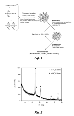
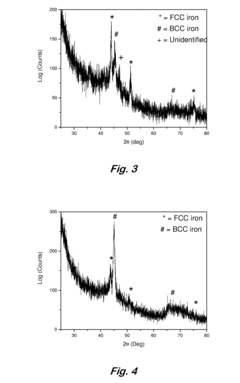
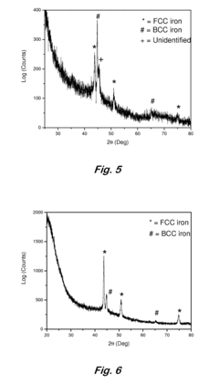
Pyrolytic formation of metallic nanoparticles
PatentActiveUS20080227624A1
Innovation
- A method involving the pyrolysis of diacetylene-containing siloxane polymers at ambient pressure to produce magnetic semiconductors like Fe0.9Co0.1Si and Fe0.1Mn0.9Si, allowing for the formation of metallic nanoparticles and tunable properties by controlling thermal energy and processing conditions.
Non-linear spin-orbit interaction devices and methods for current-to-spin conversion and amplification of spin-polarizations
PatentWO2017098363A1
Innovation
- A spin-orbit coupled device with a confinement part and circuitry that subjects charge carriers to non-linear spin-orbit interactions, allowing for rotation of spin-polarizations based on momenta and conversion of electrical current into spin-polarizations, and a spin-amplification system that utilizes a spin-to-current converter to inject and amplify spin-polarizations.


Supply Chain Analysis for Spintronic Materials
The spintronic materials supply chain represents a complex ecosystem spanning from raw material extraction to device manufacturing. Critical materials for spintronic applications include rare earth elements, transition metals, and various semiconductor materials that exhibit desirable magnetic properties. The supply chain begins with mining operations predominantly concentrated in China, Australia, and parts of Africa, creating potential geopolitical vulnerabilities for manufacturers outside these regions.
Processing of these materials requires specialized equipment and expertise, with Japan, South Korea, and Germany emerging as key players in refining technologies. The mid-stream segment involves the production of thin films, multilayer structures, and nanoscale materials that form the foundation of spintronic devices. This segment is characterized by high technical barriers to entry and significant intellectual property considerations.
Fabrication facilities for spintronic materials require ultra-clean environments and precision equipment, resulting in capital-intensive operations that favor established semiconductor manufacturers. Companies like Applied Materials, Tokyo Electron, and ASML provide essential equipment for spintronic material deposition and patterning, creating additional dependencies in the supply chain.
Recent global disruptions have highlighted vulnerabilities in the spintronic materials supply chain. The COVID-19 pandemic exposed logistical weaknesses, while geopolitical tensions between major technology-producing nations have accelerated efforts toward supply chain diversification and localization. These challenges are particularly acute for spintronic materials due to their specialized nature and limited substitutability.
Sustainability concerns are increasingly influencing supply chain decisions. The extraction of rare earth elements often involves environmentally damaging processes, prompting research into alternative materials and recycling technologies. Several companies are developing closed-loop systems to recover valuable materials from end-of-life electronic devices containing spintronic components.
Vertical integration strategies are becoming more prevalent among major manufacturers seeking to secure reliable material supplies. Companies like Samsung, Intel, and TSMC are investing in upstream capabilities or forming strategic partnerships with material suppliers to ensure consistent quality and availability of spintronic materials.
The future resilience of the spintronic materials supply chain will depend on technological innovations that reduce dependence on scarce materials, development of alternative sourcing strategies, and international cooperation frameworks that ensure stable access to critical resources while addressing environmental and ethical considerations.
Investment Trends in Spintronic Research and Development
Investment in spintronic research and development has shown significant growth over the past decade, reflecting the increasing recognition of this technology's potential to revolutionize computing and data storage. Venture capital funding in spintronic startups has increased at a compound annual growth rate of approximately 23% since 2015, with total investments exceeding $2.8 billion globally by the end of 2022.
Major technology corporations have substantially increased their R&D allocations for spintronics, with companies like IBM, Samsung, and Intel collectively investing over $1.5 billion annually in spintronic technologies. This corporate investment has been primarily directed toward memory applications, particularly Magnetoresistive Random Access Memory (MRAM) development, which has attracted approximately 60% of total spintronic funding.
Government funding has emerged as another crucial investment source, with the United States, European Union, Japan, and China implementing strategic initiatives to advance spintronic research. The EU's Horizon Europe program has allocated €450 million specifically for spintronic research between 2021-2027, while the U.S. Department of Defense has invested heavily in spintronics for radiation-hardened computing applications.
Investment patterns reveal a shifting focus from fundamental research toward commercialization efforts. Early-stage funding dominated the landscape from 2010-2015, but since 2018, later-stage investments and corporate acquisitions have increased substantially. This transition indicates the technology's maturation and growing commercial viability, particularly in specialized memory applications.
Regional analysis shows Asia-Pacific leading in spintronic manufacturing investments, with South Korea and Taiwan establishing specialized fabrication facilities. North America maintains leadership in fundamental research funding, while European investments focus heavily on quantum spintronics applications and neuromorphic computing implementations.
The investment landscape also reveals emerging specialization trends. Funding for spintronic sensors has grown at 31% annually since 2019, outpacing memory applications. Investment in spintronic-based quantum computing has seen explosive growth, with funding increasing nearly five-fold between 2018 and 2022, albeit from a smaller base.
Return on investment timelines remain challenging for investors, with typical commercialization pathways requiring 7-10 years from initial research to market entry. This extended timeline has prompted innovative funding models, including public-private partnerships and consortium-based approaches that distribute risk across multiple stakeholders while accelerating technology transfer from research institutions to commercial applications.
Unlock deeper insights with Patsnap Eureka Quick Research — get a full tech report to explore trends and direct your research. Try now!
Generate Your Research Report Instantly with AI Agent
Supercharge your innovation with Patsnap Eureka AI Agent Platform!