Understanding the EUV Lithography Process for Semiconductors
OCT 14, 20259 MIN READ
Generate Your Research Report Instantly with AI Agent
Patsnap Eureka helps you evaluate technical feasibility & market potential.
EUV Lithography Evolution and Objectives
Extreme Ultraviolet (EUV) lithography represents a revolutionary advancement in semiconductor manufacturing, emerging from decades of research and development efforts to overcome the physical limitations of traditional optical lithography. The technology's evolution began in the 1980s with initial research into short-wavelength lithography techniques, but significant breakthroughs only materialized in the early 2000s when ASML, in collaboration with Carl Zeiss and Cymer, developed the first viable EUV light sources and optical systems.
The fundamental shift from 193nm deep ultraviolet (DUV) to 13.5nm EUV wavelength marked a critical inflection point in semiconductor fabrication capabilities. This 14-fold reduction in wavelength has enabled the industry to continue following Moore's Law despite reaching what many considered insurmountable physical barriers. The progression from concept to commercial implementation spanned nearly three decades, highlighting the extraordinary technical challenges involved.
EUV lithography's primary objective is to enable high-volume manufacturing of semiconductor devices with feature sizes below 7nm, extending to 3nm and potentially beyond. This capability is essential for advancing computational power, energy efficiency, and functionality in next-generation electronic devices. Secondary objectives include reducing multi-patterning steps required in DUV lithography, thereby simplifying the manufacturing process while improving yield and reducing costs per transistor.
The technology aims to achieve resolution capabilities below 8nm half-pitch with acceptable throughput rates exceeding 125 wafers per hour to meet commercial viability requirements. Current systems have demonstrated the ability to produce 20nm features in a single exposure, with ongoing research focused on reaching sub-10nm resolution through improvements in resist chemistry, mask technology, and optical systems.
From an industry perspective, EUV lithography serves as the cornerstone technology enabling the continuation of semiconductor scaling for at least the next decade. The roadmap for EUV development includes increasing source power from current levels of approximately 250W to over 500W, improving mask defect inspection and repair capabilities, and developing high-sensitivity, low-line edge roughness photoresists specifically optimized for EUV wavelengths.
The long-term trajectory points toward High-NA (numerical aperture) EUV systems, currently under development, which promise to extend resolution capabilities even further through improved optical designs. These systems represent the next evolutionary step, potentially enabling semiconductor manufacturing at the 2nm node and beyond, though significant technical hurdles remain in areas of source power, mask infrastructure, and resist performance.
Semiconductor Market Demand Analysis
The semiconductor industry has witnessed unprecedented growth in recent years, driven primarily by the increasing demand for advanced computing capabilities across various sectors. The global semiconductor market reached approximately $556 billion in 2021 and is projected to exceed $1 trillion by 2030, representing a compound annual growth rate (CAGR) of around 7%. This remarkable expansion underscores the critical importance of advanced manufacturing technologies like Extreme Ultraviolet (EUV) lithography.
The demand for EUV lithography is particularly pronounced in the production of cutting-edge semiconductor devices with node sizes of 7nm and below. Market analysis indicates that the transition to these advanced nodes is accelerating, with major foundries and integrated device manufacturers (IDMs) investing heavily in EUV technology. This shift is primarily driven by the need for higher transistor densities to support applications in artificial intelligence, high-performance computing, and 5G/6G telecommunications.
Consumer electronics continue to be the largest end-use market for advanced semiconductors, accounting for approximately 32% of total semiconductor consumption. However, automotive and industrial applications are emerging as significant growth drivers, with projected CAGRs of 11% and 9% respectively through 2025. The automotive sector's transition toward electric vehicles and autonomous driving systems has dramatically increased the demand for high-performance computing chips manufactured using advanced lithography processes.
Geographically, East Asia dominates semiconductor manufacturing, with Taiwan, South Korea, and Japan collectively accounting for over 70% of global advanced semiconductor production. However, recent supply chain disruptions have prompted significant investments in semiconductor manufacturing capabilities in the United States and Europe, potentially reshaping the market landscape for EUV lithography equipment and services.
The memory segment, particularly DRAM and NAND flash, represents another substantial market for EUV lithography. As data centers expand to support cloud computing and AI workloads, the demand for high-density, high-performance memory chips continues to grow at approximately 15% annually. EUV lithography enables the production of memory chips with smaller feature sizes and higher bit densities, directly addressing this market need.
Industry forecasts suggest that by 2025, over 60% of leading-edge logic chips and 30% of advanced memory devices will be manufactured using EUV lithography processes. This transition represents a significant market opportunity for EUV equipment manufacturers, materials suppliers, and service providers, with the total addressable market for EUV-related products and services expected to reach $20 billion annually by mid-decade.
EUV Technology Status and Barriers
Extreme Ultraviolet (EUV) lithography represents the most advanced semiconductor manufacturing technology currently available, operating at a 13.5nm wavelength. The global implementation of EUV technology remains highly concentrated, with only a handful of companies possessing the capability to deploy it at scale. ASML maintains a virtual monopoly on EUV lithography equipment manufacturing, while Samsung, TSMC, and Intel lead in implementation for high-volume manufacturing.
Despite significant progress, EUV lithography faces substantial technical barriers. Power source stability remains a critical challenge, with current EUV light sources struggling to maintain consistent high power levels needed for production efficiency. The industry standard aims for 250W sources, but maintaining this output reliably over extended production runs continues to challenge manufacturers. This power limitation directly impacts throughput, creating a significant economic barrier to wider adoption.
Mask defectivity presents another major obstacle. EUV masks are extraordinarily complex multilayer structures that must be virtually defect-free. Even microscopic imperfections can result in critical pattern failures. The industry continues to work on improving mask inspection tools and defect mitigation strategies, but this remains a yield-limiting factor.
Photoresist performance constitutes a third critical barrier. EUV photoresists must simultaneously achieve high sensitivity (to compensate for limited source power), high resolution, and low line edge roughness - a challenging set of requirements often referred to as the "triangle trade-off." Current photoresist technologies still struggle to optimize these competing parameters without compromise.
Stochastic effects represent perhaps the most fundamental physical limitation of EUV lithography. At extreme dimensions, random variations in photon absorption and chemical reactions within the photoresist become significant, leading to unpredictable pattern variations. These effects become increasingly pronounced as feature sizes approach sub-10nm dimensions, threatening the continued scaling promised by EUV.
Infrastructure requirements present substantial economic barriers. The implementation of EUV lithography demands specialized cleanroom environments, extensive vibration control systems, and vacuum infrastructure. The capital expenditure for a single EUV lithography tool exceeds $150 million, with additional costs for supporting infrastructure.
Geographically, EUV technology development remains concentrated in a few regions. The Netherlands dominates equipment manufacturing through ASML, while Japan (Canon, Nikon) and the United States (Intel) maintain significant research activities. Implementation is primarily occurring in Taiwan (TSMC), South Korea (Samsung), and the United States (Intel), creating potential geopolitical vulnerabilities in the semiconductor supply chain.
Current EUV Implementation Solutions
01 EUV Lithography System Design and Components
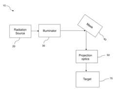
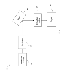
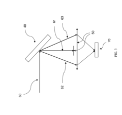
EUV lithography systems incorporate specialized components designed to work with extreme ultraviolet light. These systems typically include radiation sources, illumination optics, projection optics, and wafer stages. The design focuses on optimizing the optical path to maintain beam quality while minimizing energy loss. Advanced components such as mirrors with multilayer coatings are used instead of traditional lenses due to the high absorption of EUV radiation by most materials.- EUV lithography system design and components: EUV lithography systems incorporate specialized components designed to work with extreme ultraviolet light. These systems include illumination optics, projection optics, and reflective masks that operate in vacuum environments. The design focuses on achieving high resolution patterning while managing the challenges of working with short wavelength EUV radiation. Advanced optical elements and precise positioning mechanisms are essential for maintaining imaging accuracy at nanometer scales.
- Contamination control in EUV lithography: Contamination control is critical in EUV lithography due to the sensitivity of optical components to molecular and particulate contamination. Methods include specialized cleaning techniques, protective pellicles, and environmental control systems to prevent carbon growth on mirrors and masks. Hydrogen and other gas purging techniques are employed to reduce contamination and extend the lifetime of expensive optical components, ensuring consistent lithographic performance.
- EUV source technology and power optimization: EUV light sources typically use laser-produced plasma or discharge-produced plasma to generate the required 13.5nm wavelength radiation. Innovations focus on increasing source power while maintaining stability, as source power directly impacts throughput in semiconductor manufacturing. Technologies include tin droplet targets, laser pulse optimization, and collector mirror designs that maximize EUV light collection efficiency while managing thermal loads and debris mitigation.
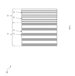
- Mask technology for EUV lithography: EUV masks are fundamentally different from traditional photomasks, using reflective rather than transmissive designs. They consist of multilayer mirrors with absorber patterns on top. Innovations include defect inspection and repair techniques, pattern placement accuracy improvements, and methods to reduce mask-induced imaging errors. Advanced mask designs incorporate phase shifting elements and assist features to enhance resolution and process windows for critical semiconductor features.
- Computational lithography for EUV processes: Computational methods are essential for optimizing EUV lithography processes. These include optical proximity correction, source mask optimization, and inverse lithography techniques tailored for EUV's unique imaging characteristics. Advanced modeling accounts for stochastic effects that become significant at EUV wavelengths. Machine learning algorithms are increasingly applied to predict and compensate for process variations, improving pattern fidelity and yield in high-volume manufacturing environments.
02 Contamination Control in EUV Lithography
Contamination control is critical in EUV lithography due to the sensitivity of the process to even microscopic particles. Various methods are employed to prevent and mitigate contamination, including specialized cleaning techniques, protective pellicles, and environmental control systems. Hydrogen and other gases are often used to clean optical surfaces and prevent carbon buildup. Vacuum systems are implemented to reduce particle presence in the optical path.Expand Specific Solutions03 EUV Mask Technology and Defect Management
EUV masks require specialized technology due to the reflective nature of EUV lithography. These masks typically consist of multilayer reflective coatings with absorber patterns. Defect management is crucial as even nanometer-scale imperfections can affect pattern transfer. Advanced inspection techniques are employed to detect and characterize defects, while repair methods help to mitigate their impact on the final printed pattern.Expand Specific Solutions04 EUV Source Technology and Power Optimization
EUV radiation sources typically use laser-produced plasma or discharge-produced plasma technologies. These sources generate EUV light by exciting tin or other materials to create high-energy plasma. Power optimization is a critical challenge, as sufficient power is needed for high-volume manufacturing while maintaining source stability and component lifetime. Various techniques are employed to increase conversion efficiency and reduce debris generation.Expand Specific Solutions05 Computational Methods for EUV Lithography
Computational methods play a crucial role in EUV lithography, including optical proximity correction, source mask optimization, and inverse lithography techniques. These methods help to compensate for process variations and optical effects that can impact pattern fidelity. Machine learning and artificial intelligence approaches are increasingly being applied to optimize EUV processes, predict defects, and enhance overall system performance.Expand Specific Solutions
Leading EUV Equipment Manufacturers and Ecosystem
The EUV lithography market is in a growth phase, with increasing adoption for advanced semiconductor manufacturing. The market size is expanding rapidly, driven by demand for smaller, more powerful chips. Technologically, ASML Netherlands BV dominates as the sole supplier of EUV lithography systems, while Taiwan Semiconductor Manufacturing Co. and Samsung Electronics lead in implementation. Other key players include Applied Materials, Tokyo Electron, and KLA TENCOR providing complementary tools and services. The ecosystem also includes materials suppliers like DuPont and optical specialists such as Carl Zeiss SMT. This competitive landscape reflects the high barriers to entry and specialized expertise required in this critical semiconductor manufacturing technology.
Taiwan Semiconductor Manufacturing Co., Ltd.
Technical Solution: TSMC has pioneered the implementation of EUV lithography in high-volume manufacturing, being the first to use this technology for 7nm+ and 5nm process nodes[1]. Their approach integrates EUV into a hybrid lithography strategy, using EUV for critical layers that require the highest resolution while employing multi-patterning techniques with traditional immersion lithography for other layers[2]. TSMC has developed specialized photoresist materials optimized for EUV sensitivity and resolution in partnership with suppliers. Their process includes advanced computational lithography techniques to optimize mask designs specifically for EUV characteristics. TSMC has implemented unique solutions for managing EUV-specific challenges including stochastic effects and pattern roughness through proprietary design rules and process control methods[3]. They've also created custom metrology and inspection workflows to ensure quality control in EUV-patterned layers, achieving defect densities below 0.01 defects/cm² at critical layers[4]. TSMC's N5 and N3 process nodes leverage EUV extensively, with N3 reportedly using up to 25+ EUV layers.
Strengths: Industry-leading implementation expertise with proven high-volume manufacturing capability; comprehensive process integration knowledge; advanced defect control and yield management systems specific to EUV. Weaknesses: Heavy dependence on ASML as the sole EUV equipment supplier; extremely high capital investment requirements; challenges in scaling EUV implementation to meet growing demand across multiple technology nodes simultaneously.
Samsung Electronics Co., Ltd.
Technical Solution: Samsung has developed a comprehensive EUV implementation strategy that spans both memory and logic semiconductor production. Their approach includes a specialized EUV process that utilizes single-exposure patterning for critical dimensions down to 20nm, significantly reducing process complexity compared to multiple patterning techniques[1]. Samsung's EUV implementation features custom-developed photoresists with sensitivity optimized for their specific process requirements, achieving exposure doses around 20mJ/cm² while maintaining pattern fidelity[2]. They've pioneered the use of EUV for DRAM production, being the first to implement it in their 1z-nm DRAM process. For logic, Samsung's 7nm and 5nm processes incorporate extensive EUV usage, with their 3nm GAA (Gate-All-Around) technology utilizing EUV for up to 30 critical layers[3]. Samsung has developed proprietary computational lithography techniques specifically for EUV, including source mask optimization and optical proximity correction algorithms tailored to the unique optical characteristics of EUV wavelengths. Their approach also includes advanced metrology systems for EUV-specific defect detection and process control[4].
Strengths: Vertically integrated approach with both equipment expertise and manufacturing implementation; broad application across both memory and logic products; significant R&D resources dedicated to EUV process optimization. Weaknesses: Slightly behind TSMC in high-volume manufacturing maturity for leading-edge nodes; challenges in achieving consistent yields across diverse product portfolio; high capital intensity required for maintaining competitive position.
Critical EUV Patents and Technical Innovations
Extreme Ultraviolet Lithography Process and Mask
PatentActiveUS20150168845A1
Innovation
- The implementation of a nearly on-axis illumination with partial coherence less than 0.3 in an EUV lithography system, combined with an EUV mask featuring a first region with main polygons and a second region with sub-resolution polygons, and a spatial filter to remove most non-diffracted light, enhancing spatial frequency resolution and uniformity of exposure intensity.
Extreme ultraviolet lithography process and mask
PatentInactiveUS9529272B2
Innovation
- The EUV lithography process employs nearly complete on-axis illumination with partial coherence less than 0.3, utilizing a pupil filter to remove over 70% of non-diffracted lights and filter out reflected lights from assist polygons, while using an EUV mask with multiple states assigned to adjacent polygons and assist polygons, and a projection optics box to collect and direct diffracted lights for improved imaging.


Supply Chain Resilience for EUV Components
The EUV lithography supply chain represents one of the most complex and vulnerable aspects of advanced semiconductor manufacturing. The highly specialized nature of EUV components creates significant resilience challenges, with many critical parts having single-source suppliers. ASML, as the sole manufacturer of EUV lithography machines, relies on a network of approximately 5,000 suppliers across three continents, creating multiple potential points of failure.
Key components like the laser-produced plasma source require specialized materials including rare gases and precise optical elements that often have limited sourcing options. The ultra-precise mirrors coated with multilayer reflective materials represent another critical vulnerability, as their production requires extraordinary manufacturing precision that few companies worldwide can achieve.
Geographic concentration presents additional resilience challenges. Many essential EUV components originate from specific regions, creating geopolitical dependencies. For instance, certain specialized chemicals come predominantly from Japan, while advanced optical systems rely heavily on European manufacturers. This geographic specialization increases vulnerability to regional disruptions, whether from natural disasters, political tensions, or public health emergencies.
Recent global events have highlighted these vulnerabilities. The COVID-19 pandemic caused significant delays in EUV equipment delivery, while trade tensions between major economies have raised concerns about technology access restrictions. Semiconductor manufacturers have responded by implementing various resilience strategies, including increased inventory buffers for critical components and development of alternative supplier relationships where possible.
Industry leaders are exploring several approaches to enhance supply chain resilience. Vertical integration efforts aim to bring critical component production in-house, reducing external dependencies. Collaborative industry initiatives focus on developing redundant supply sources for the most vulnerable components. Additionally, geographic diversification strategies seek to distribute manufacturing capabilities across multiple regions to mitigate regional disruption risks.
Looking forward, the industry must balance the efficiency benefits of specialized supply chains against resilience requirements. This may necessitate accepting higher costs and potential inefficiencies to ensure manufacturing continuity. As EUV lithography becomes increasingly central to advanced semiconductor production, securing this complex supply chain will remain a critical priority for the entire semiconductor ecosystem.
Environmental Impact of EUV Manufacturing
The environmental footprint of Extreme Ultraviolet (EUV) lithography represents a significant consideration in semiconductor manufacturing sustainability. EUV systems consume substantial energy, with each lithography tool requiring between 500-1000 kW during operation—approximately 10 times more than previous generation deep ultraviolet (DUV) systems. This increased power demand stems primarily from the complex laser-produced plasma process needed to generate EUV light, where tin droplets are vaporized by high-powered CO2 lasers.
Water usage presents another critical environmental concern. A single EUV lithography tool can consume 1,500-3,000 liters of ultra-pure water daily for cooling systems and cleaning processes. The purification of this water requires additional energy inputs and chemical treatments, creating a compound environmental impact beyond the direct manufacturing process.
Chemical consumption in EUV manufacturing introduces further environmental challenges. The photoresist materials used in EUV lithography often contain metal-organic compounds and fluorinated substances with potential environmental persistence. Additionally, the cleaning and maintenance of EUV systems require specialized solvents and gases, some with high global warming potential (GWP) values exceeding 10,000 times that of CO2.
Waste management represents an ongoing challenge for the semiconductor industry adopting EUV technology. The tin debris from the plasma source requires specialized handling and disposal protocols. Furthermore, used photoresist materials, contaminated filters, and other consumables generate hazardous waste streams that necessitate careful treatment and disposal.
Several leading semiconductor manufacturers have initiated sustainability programs specifically addressing EUV environmental impacts. ASML, the primary manufacturer of EUV lithography equipment, has committed to improving energy efficiency by 60% per wafer pass by 2025 compared to 2018 baselines. Similarly, companies like TSMC and Samsung have announced circular economy initiatives to recycle cooling water and recover valuable materials from EUV-related waste streams.
Regulatory frameworks worldwide are evolving to address the environmental implications of advanced semiconductor manufacturing. The European Union's Restriction of Hazardous Substances (RoHS) and Registration, Evaluation, Authorization and Restriction of Chemicals (REACH) regulations increasingly scrutinize materials used in EUV processes. Meanwhile, carbon pricing mechanisms in various regions are creating economic incentives for reducing the energy intensity of semiconductor manufacturing.
Looking forward, the industry is exploring several promising approaches to mitigate EUV's environmental impact, including more efficient EUV light sources, closed-loop water recycling systems, and alternative photoresist chemistries with reduced environmental persistence. These innovations will be crucial as EUV lithography deployment expands globally in the coming decade.
Unlock deeper insights with Patsnap Eureka Quick Research — get a full tech report to explore trends and direct your research. Try now!
Generate Your Research Report Instantly with AI Agent
Supercharge your innovation with Patsnap Eureka AI Agent Platform!