

Why EUV Lithography Outpaces Traditional Methods in Precision
OCT 14, 20259 MIN READ
Generate Your Research Report Instantly with AI Agent
PatSnap Eureka helps you evaluate technical feasibility & market potential.
EUV Lithography Evolution and Precision Goals
Extreme Ultraviolet (EUV) lithography represents a revolutionary advancement in semiconductor manufacturing, emerging after decades of research and development efforts to overcome the physical limitations of traditional optical lithography methods. The evolution of lithography technology has been driven by the semiconductor industry's relentless pursuit of Moore's Law, which predicted the doubling of transistor density approximately every two years. Traditional deep ultraviolet (DUV) lithography, using 193nm wavelength light, reached its theoretical limits around the 45nm node, necessitating complex multi-patterning techniques to achieve smaller feature sizes.
EUV lithography, operating at a dramatically shorter wavelength of 13.5nm, emerged as the most promising solution to continue semiconductor scaling. The technology's development timeline spans over three decades, beginning with fundamental research in the 1990s, followed by the formation of industry consortia in the early 2000s, and culminating in the first commercial deployment by ASML in 2019. This extended development period reflects the enormous technical challenges involved in creating a viable EUV ecosystem.
The precision goals of EUV lithography are directly tied to the semiconductor industry's roadmap for advanced node development. Current EUV systems target feature sizes below 7nm, with future iterations aiming to enable 3nm and smaller nodes. This unprecedented level of precision requires extraordinary engineering achievements across multiple domains, including optics, materials science, and mechanical systems.
A key technical objective of EUV lithography is to achieve higher numerical aperture (NA) values, with next-generation systems targeting NA values of 0.55 compared to current 0.33 NA systems. This advancement promises to further enhance resolution capabilities while maintaining acceptable depth of focus for manufacturing processes. Additionally, EUV technology aims to increase wafer throughput from current levels of approximately 140 wafers per hour to over 185 wafers per hour, addressing economic viability concerns.
The evolution of EUV technology has been characterized by continuous improvements in source power, from early experimental systems producing less than 10W to current production systems exceeding 250W. Future roadmaps target 500W sources to further enhance throughput and reduce cost-per-layer metrics. Concurrent advancements in resist chemistry, mask technology, and defect inspection capabilities have been essential complementary developments.
Looking forward, the industry is exploring potential extensions to EUV technology, including high-NA EUV systems and novel patterning approaches that combine EUV with directed self-assembly or selective deposition techniques. These evolutionary paths aim to extend semiconductor scaling well into the next decade, potentially enabling feature sizes approaching atomic dimensions.
Market Demand for Advanced Semiconductor Fabrication
The semiconductor industry has witnessed an unprecedented surge in demand for advanced fabrication technologies, primarily driven by the relentless pursuit of Moore's Law and the increasing complexity of integrated circuits. Market research indicates that the global semiconductor manufacturing equipment market reached approximately $103 billion in 2022, with lithography systems accounting for nearly 30% of this value. This substantial market share underscores the critical importance of lithography in semiconductor fabrication processes.
The demand for EUV lithography specifically has been accelerating due to several converging market forces. Leading semiconductor manufacturers like TSMC, Samsung, and Intel have committed billions to EUV implementation in their advanced node production lines. TSMC alone invested over $20 billion in capital expenditure in 2022, with a significant portion allocated to EUV lithography equipment for their 5nm and 3nm process nodes.
Consumer electronics continue to drive significant demand for smaller, more powerful chips. The smartphone market, despite reaching maturity in developed regions, still requires annual advancements in processor capabilities, creating consistent demand for cutting-edge fabrication technologies. Additionally, the explosive growth in artificial intelligence and machine learning applications has created unprecedented demand for specialized high-performance chips that can only be manufactured using the most advanced lithography techniques.
The automotive sector represents another rapidly expanding market for advanced semiconductors. Modern vehicles incorporate dozens of microprocessors and specialized chips for everything from engine management to advanced driver assistance systems. As autonomous driving technologies mature, the demand for sophisticated chips manufactured using precision lithography will continue to grow substantially.
Data center expansion represents yet another major driver for advanced semiconductor fabrication. The global shift toward cloud computing, coupled with increasing data storage and processing requirements, has led to massive investments in data center infrastructure. These facilities require high-performance, energy-efficient processors that can only be manufactured using the most advanced lithography techniques.
Market analysts project that the EUV lithography equipment market will grow at a compound annual growth rate of 21.5% through 2027. This growth trajectory reflects not only the technical superiority of EUV technology but also the expanding applications across multiple industries. The Internet of Things, 5G/6G telecommunications infrastructure, and quantum computing research all contribute to sustained demand for increasingly sophisticated semiconductor manufacturing capabilities.
The geographical distribution of this demand is also evolving, with significant investments in semiconductor manufacturing capacity occurring in the United States, Europe, and various Asian countries as governments recognize the strategic importance of domestic chip production capabilities.
EUV vs Traditional Lithography: Current Capabilities and Limitations
Extreme Ultraviolet (EUV) lithography represents a revolutionary advancement in semiconductor manufacturing, operating at a wavelength of 13.5nm compared to the 193nm used in traditional Deep Ultraviolet (DUV) immersion lithography. This significant wavelength reduction enables EUV to achieve unprecedented precision in pattern transfer, allowing for the creation of semiconductor features below 7nm—a threshold that traditional methods struggle to reach efficiently.
Traditional lithography techniques have reached their physical limits despite numerous enhancement strategies. ArF immersion lithography, the most advanced conventional method, employs liquid immersion and multi-patterning techniques to extend its capabilities. However, these approaches introduce additional process steps, increasing manufacturing complexity, time, and cost. The resolution enhancement techniques (RETs) like optical proximity correction and phase-shift masks add further complexity without fundamentally solving the wavelength limitation.
EUV lithography demonstrates superior resolution capabilities, achieving feature sizes down to 13nm in single exposure processes where traditional methods would require quadruple patterning. This translates to significantly higher transistor densities on chips, enabling continued adherence to Moore's Law. The single-exposure capability of EUV for advanced nodes dramatically reduces mask layers—from 80+ with multi-patterning DUV to approximately 20 with EUV—simplifying the manufacturing process substantially.
Despite its advantages, EUV technology faces several limitations. Power source efficiency remains a challenge, with current EUV systems utilizing only about 5% of input power for actual lithography. This inefficiency contributes to the high operational costs of EUV systems, which can exceed $150 million per tool. Additionally, EUV requires specialized vacuum environments and reflective optics rather than the transmissive lenses used in traditional lithography, adding complexity to the manufacturing infrastructure.
Defectivity control presents another significant challenge for EUV. The technology's extreme sensitivity means that even minuscule mask defects or contamination can cause critical pattern failures. Traditional lithography benefits from decades of defect management experience, while EUV defect inspection and repair technologies are still evolving.
Throughput comparison reveals that current EUV systems process approximately 140 wafers per hour, while advanced DUV immersion tools can handle up to 275 wafers per hour. This throughput gap is gradually narrowing as EUV technology matures, but it remains a consideration for high-volume manufacturing environments where production speed directly impacts cost-effectiveness.
The economic equation balances in favor of EUV for advanced nodes below 7nm, where the reduction in process steps outweighs the higher equipment costs. For less advanced nodes, traditional lithography maintains cost advantages, creating a bifurcated manufacturing landscape where both technologies coexist, each serving different segments of the semiconductor market.
Technical Architecture of Modern EUV Lithography Systems
01 Optical system optimization for EUV lithography
Optimization of optical systems in EUV lithography involves precise alignment and calibration of mirrors, lenses, and other optical components to achieve nanometer-scale precision. Advanced optical designs minimize aberrations and distortions that could affect pattern transfer accuracy. These systems often incorporate adaptive optics and feedback mechanisms to maintain optimal performance during the lithography process, compensating for thermal effects and mechanical vibrations that could degrade precision.- Optical system optimization for EUV lithography: Optical systems in EUV lithography can be optimized to enhance precision through various techniques. These include advanced mirror designs, optical aberration correction systems, and specialized lens arrangements that minimize distortion. By improving the optical path and reducing wavefront errors, these systems can achieve higher resolution and better pattern fidelity in the nanometer range, which is crucial for next-generation semiconductor manufacturing.
- Alignment and positioning systems for EUV precision: Precise alignment and positioning systems are essential for EUV lithography accuracy. These systems incorporate advanced sensors, interferometric measurement techniques, and feedback control mechanisms to achieve nanometer-level positioning precision. By minimizing stage vibration and implementing real-time position correction, these technologies ensure accurate pattern overlay and registration, which directly impacts the quality and reliability of fabricated semiconductor devices.
- Thermal management for EUV lithography stability: Thermal management is critical for maintaining precision in EUV lithography systems. Specialized cooling systems, temperature-controlled environments, and thermally stable materials help minimize thermal expansion and contraction that could affect dimensional accuracy. Advanced thermal compensation algorithms and active temperature control mechanisms work together to maintain system stability during the high-energy EUV exposure process, ensuring consistent pattern reproduction.
- Mask and reticle technologies for enhanced EUV precision: Advanced mask and reticle technologies significantly impact EUV lithography precision. These include phase-shifting masks, optical proximity correction features, and specialized absorber materials that enhance pattern fidelity. Innovations in mask fabrication, inspection, and repair techniques help minimize defects that could compromise lithographic precision. Multi-layer reflective mask structures are specifically designed to maximize EUV light utilization while maintaining critical dimension control.
- Computational lithography and error correction methods: Computational lithography and error correction methods enhance EUV precision through software-based approaches. These include advanced modeling algorithms, machine learning techniques for pattern prediction, and inverse lithography technology that optimizes mask designs. Source mask optimization and optical proximity correction algorithms compensate for systematic process variations. Real-time feedback systems analyze and correct errors during exposure, pushing the boundaries of achievable resolution and pattern fidelity in EUV lithography.
02 Mask and reticle technology for EUV precision
Advanced mask and reticle technologies are critical for EUV lithography precision. These components feature specialized multilayer coatings that reflect EUV radiation with high efficiency. Sophisticated pattern correction techniques compensate for optical proximity effects and other distortions. The manufacturing process for these masks requires atomic-level precision to ensure accurate pattern transfer to the wafer, with innovative inspection and repair methods to identify and address defects that could impact lithographic precision.Expand Specific Solutions03 Positioning and alignment systems for nanometer precision
Achieving nanometer-level precision in EUV lithography requires sophisticated positioning and alignment systems. These systems incorporate interferometric measurement techniques, advanced servo control mechanisms, and real-time feedback loops to maintain precise positioning of the wafer and mask. Multi-axis stage systems with vibration isolation capabilities ensure stable positioning during exposure. Alignment marks and detection systems enable accurate overlay between multiple lithography steps, which is essential for complex semiconductor device fabrication.Expand Specific Solutions04 Environmental control for EUV lithography stability
Environmental factors significantly impact EUV lithography precision. Advanced systems incorporate vacuum environments to prevent EUV radiation absorption and contamination. Temperature control systems maintain thermal stability to prevent expansion and contraction of components. Specialized shielding protects against electromagnetic interference that could affect positioning accuracy. Contamination control measures prevent particles from degrading mask and optical surfaces. These environmental control systems work together to create stable conditions necessary for consistent nanometer-scale pattern transfer.Expand Specific Solutions05 Computational methods for enhancing EUV precision
Computational techniques play a crucial role in enhancing EUV lithography precision. Advanced modeling and simulation tools predict and compensate for process variations. Optical proximity correction algorithms adjust mask patterns to account for diffraction effects. Machine learning approaches optimize process parameters based on historical data. Real-time computational systems process sensor data to make dynamic adjustments during exposure. These computational methods enable finer control over the lithography process, helping to achieve the extreme precision required for advanced semiconductor manufacturing.Expand Specific Solutions
Key Industry Players in EUV Lithography Ecosystem
EUV lithography represents a transformative advancement in semiconductor manufacturing, currently in its growth phase with expanding market adoption. The technology offers unprecedented precision at sub-7nm nodes, significantly outperforming traditional DUV methods. Market leaders ASML Holding dominates the EUV equipment sector, while Taiwan Semiconductor Manufacturing Co. (TSMC), Samsung Electronics, and Intel are driving implementation in high-volume production. The competitive landscape includes established players like Nikon and emerging Chinese entities such as SMIC and Shanghai Micro Electronics Equipment, though they lag in technological maturity. With the global semiconductor market increasingly dependent on advanced nodes, EUV technology's estimated $10+ billion market continues to grow as chipmakers invest heavily in this critical manufacturing capability.
Taiwan Semiconductor Manufacturing Co., Ltd.
Technical Solution: TSMC has pioneered the implementation of EUV lithography in high-volume manufacturing, beginning with their 7nm+ process and expanding to 5nm and 3nm nodes. Their approach integrates EUV with multi-patterning techniques to achieve unprecedented transistor densities of over 100 million transistors per square millimeter at 5nm. TSMC's EUV implementation reduces mask layers by approximately 20% compared to traditional multi-patterning approaches, significantly decreasing manufacturing complexity and cycle time. Their process achieves critical dimension uniformity below 1nm, enabling consistent chip performance across wafers. TSMC has developed specialized resist materials optimized for EUV exposure, improving sensitivity while maintaining resolution requirements. The company has also created advanced computational correction systems that compensate for mask 3D effects and other EUV-specific challenges, resulting in improved pattern fidelity and yield rates exceeding 90% for complex designs[2][4].
Strengths: Industry-leading implementation in high-volume manufacturing; demonstrated ability to scale to 3nm and beyond; integration expertise with complementary technologies; highest yield rates in production. Weaknesses: Extreme dependence on ASML for equipment; high capital expenditure requirements; geographic concentration risk; challenges in maintaining consistent output across multiple fabs.
Nikon Corp.
Technical Solution: While not currently a major player in EUV lithography, Nikon has developed alternative precision lithography approaches that compete with EUV in specific applications. Their NSR-S635E immersion lithography system achieves resolution down to 38nm through advanced multi-patterning techniques, offering a cost-effective alternative for less critical layers. Nikon's proprietary "Streamlign" platform incorporates computational lithography and process correction technologies that improve overlay accuracy to below 2.5nm, approaching EUV capabilities for certain applications. The company has invested in nanoimprint lithography (NIL) technology as a potential alternative to EUV for specific use cases, achieving sub-20nm resolution at significantly lower cost. Nikon maintains research programs in EUV-adjacent technologies, including directed self-assembly (DSA) and multi-beam mask writing, which complement advanced lithography processes. Their systems feature advanced alignment technologies with accuracy below 1.5nm, critical for the precise layer-to-layer registration required in advanced nodes regardless of exposure technology[9][10].
Strengths: Cost-effective solutions for less critical layers; expertise in optical systems and precision engineering; complementary technologies that enhance overall lithography ecosystem; strong position in mature nodes. Weaknesses: Limited presence in true EUV technology; declining market share in leading-edge lithography; technological gap compared to ASML's EUV capabilities; challenges in maintaining relevance for most advanced nodes.
Critical Patents and Breakthroughs in EUV Technology
Method for extreme ultraviolet lithography
PatentInactiveUS6162577A
Innovation
- Development of photoresists that are more transparent to EUV radiation, specifically single-layer and bi-layer resist schemes, where the bi-layer resist includes a planarizing layer and a thin etch-resistant imaging layer, allowing for increased resolution and sensitivity, and using a reflective mask with a Schwarzschild camera for EUV lithography.
Extreme ultraviolet lithography device and operating method thereof
PatentPendingTW202414067A
Innovation
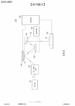
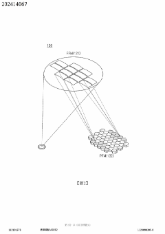
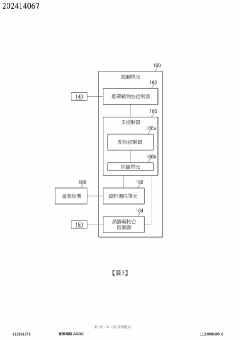
- Implementing a free-form EUV illumination system optimized through linear programming and priority optimization, using algorithms like the Hungarian method to allocate mirrors and assign priorities based on symmetry criteria, converting illumination system images into a format usable by EUV scanners.

Economic Impact and ROI Analysis of EUV Implementation
The implementation of Extreme Ultraviolet (EUV) lithography represents a significant financial investment for semiconductor manufacturers, with initial capital expenditures reaching $120-150 million per tool. Despite this substantial upfront cost, economic analyses indicate compelling long-term returns that justify the transition from traditional lithography methods.
When evaluating the economic impact of EUV implementation, manufacturers experience reduced process steps compared to multi-patterning techniques required in traditional lithography. This streamlining translates to approximately 20-30% lower production costs per wafer at advanced nodes (7nm and below), despite the higher initial investment. The simplified process flow also contributes to improved yield rates, typically increasing from 80% to over 90% for complex chip designs.
Return on investment calculations demonstrate that EUV systems typically achieve break-even within 3-5 years of implementation, depending on production volume and chip complexity. For high-volume manufacturers producing premium chips, this timeline can be further compressed to 2-3 years due to the significant margin improvements on advanced node products.
The economic benefits extend beyond direct manufacturing costs. EUV enables the continuation of Moore's Law economics, allowing chipmakers to maintain the historical 30% cost reduction per transistor with each new node. Without EUV technology, this economic trajectory would stall, threatening the industry's fundamental business model and innovation pace.
Market analysis reveals that early adopters of EUV technology have secured competitive advantages through faster time-to-market for advanced node products. These companies have captured premium pricing opportunities and established leadership positions in high-margin segments such as mobile processors, AI accelerators, and high-performance computing chips.
The broader economic impact includes significant supply chain effects, with EUV implementation creating specialized job opportunities in advanced manufacturing, process engineering, and equipment maintenance. The technology has also spurred regional economic development around semiconductor manufacturing clusters, with governments increasingly viewing EUV capability as strategic for national economic security.
Risk assessment models indicate that while EUV implementation carries substantial financial exposure, the alternative—continuing with increasingly complex multi-patterning approaches—presents even greater economic risks through diminishing returns, yield challenges, and competitive disadvantages in the rapidly evolving semiconductor marketplace.
Environmental and Resource Considerations in Advanced Lithography
The environmental impact of lithography technologies has become increasingly important as semiconductor manufacturing continues to advance. EUV lithography, while superior in precision, presents distinct environmental considerations compared to traditional lithographic methods. The chemical usage profile of EUV differs significantly from conventional techniques, with a notable reduction in photoresist materials and processing chemicals. This reduction stems from EUV's ability to create more precise patterns with fewer process steps, thereby minimizing chemical waste generation.
Water consumption represents another critical environmental factor in lithography processes. Traditional immersion lithography systems require substantial amounts of ultra-pure water, both for the immersion fluid and for cleaning processes. EUV systems, while still requiring water for cooling and maintenance, generally demonstrate improved efficiency in water utilization per wafer processed, contributing to more sustainable manufacturing practices in regions facing water scarcity challenges.
Energy consumption patterns reveal complex trade-offs between lithography technologies. EUV systems demand significant power to operate their plasma light sources, with a single EUV scanner potentially consuming 1-1.5 MW during operation. This exceeds the energy requirements of traditional DUV scanners. However, when evaluated on a per-layer basis across the entire manufacturing process, EUV's ability to reduce multi-patterning steps can potentially offset this higher direct energy consumption, resulting in comparable or even improved overall energy efficiency for complex chip designs.
Waste management considerations extend beyond chemical usage to include equipment lifecycle factors. The sophisticated components in EUV systems, particularly the complex mirror systems and specialized light sources, present unique end-of-life recycling challenges. The industry has begun developing specialized recycling protocols for these high-value components, recognizing both the environmental imperative and the economic value of recovering rare materials used in these systems.
Resource scarcity concerns are particularly relevant for EUV technology, which relies on specific rare materials for its operation. The mirrors in EUV systems require specialized coatings containing rare elements, while the plasma generation process typically uses tin. As EUV adoption accelerates, ensuring sustainable sourcing of these materials becomes increasingly important for long-term viability. Industry initiatives have emerged to address these concerns through improved material recovery systems and research into alternative materials that could reduce dependence on scarce resources.
Carbon footprint assessments of advanced lithography must consider both direct operational emissions and embodied carbon in equipment manufacturing. While EUV systems have higher embodied carbon due to their complexity, their potential to reduce the total number of process steps in semiconductor manufacturing may yield net carbon benefits when evaluated across the complete production lifecycle of advanced semiconductor devices.
Unlock deeper insights with PatSnap Eureka Quick Research — get a full tech report to explore trends and direct your research. Try now!
Generate Your Research Report Instantly with AI Agent
Supercharge your innovation with PatSnap Eureka AI Agent Platform!