Array substrate, and 3D display device and drive method thereof

A technology for an array substrate and a display device, applied in the field of 3D display, can solve the problems of low product yield of display device, reduced transmittance of display device, increase in product cost, etc., so as to achieve 3D display, ensure charging time, and reduce charging effect of time

Inactive Publication Date: 2013-03-20
BOE TECH GRP CO LTD +1
View PDF11 Cites 3 Cited by
  • Summary
  • Abstract
  • Description
  • Claims
  • Application Information

AI Technical Summary

Problems solved by technology

In order to ensure the charging rate of the pixel electrode, it is often necessary to increase the line width of the wire on the display device to reduce the load on the display device, which will reduce the transmittance of the display device; and the product yield of the display device with a high refresh rate is not high. resulting in an increase in the cost of the product

Method used


Image

  • Array substrate, and 3D display device and drive method thereof
  • Array substrate, and 3D display device and drive method thereof
  • Array substrate, and 3D display device and drive method thereof

Examples


Embodiment Construction

[0033] In order to make the technical problems, technical solutions and advantages to be solved by the embodiments of the present invention clearer, the following will describe in detail with reference to the drawings and specific embodiments.

[0034] Embodiments of the present invention provide an array substrate, a 3D display device and a driving method thereof, which can ensure the charging time of pixel electrodes while increasing the refresh frequency of the display device, and realize 3D display.

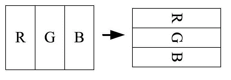
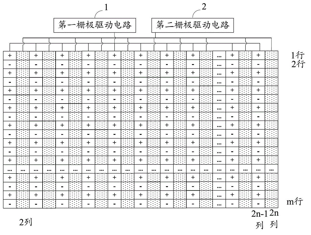
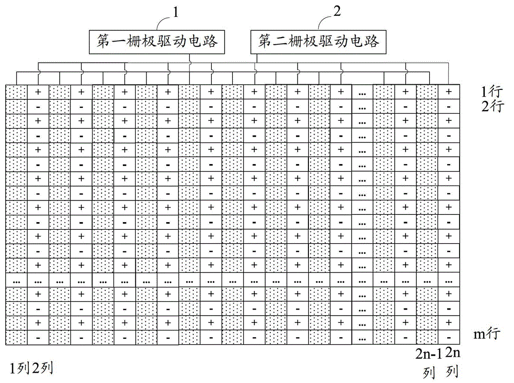
[0035] At present, the mainstream 3D format of radio and television in several major regions of the world such as mainland China is set as L / R mode: in the original 60Hz image, the signal source of each frame is half of the image for the left eye and half of the image for the right eye constituted. In order to cooperate with this display mode, an embodiment of the present invention provides an array substrate, including a substrate, m rows and 2n columns of pixel units formed...


PUM


Abstract

The invention provides an array substrate, and a 3D display device and a drive method thereof, belonging to the field of 3D display. The array substrate comprises a substrate, m lines and 2n columns of pixel units formed on the substrate by adopting a matrix mode, data lines corresponding to the m lines of pixel units and gate lines corresponding to the 2n columns of pixel units, wherein each data line is connected with a source electrode of a thin film transistor in the corresponding pixel unit, each gate line is connected with a gate electrode of the thin film transistor in the corresponding pixel unit, the gate lines are used for receiving gate electrode scanning signals according to a preset time period, the gate line corresponding to the (2k-1)th column of pixel units is used for receiving the gate electrode scanning signal within a first time quantum of the preset time period, and the gate line corresponding to the (2k)th column of pixel units is used for receiving the gate electrode scanning signal within a second time quantum of the preset time period. According to the technical scheme, the refreshing frequency of a display panel can be increased, the charging time of pixel electrodes is ensured, and the 3D display is realized.

Description

technical field [0001] The present invention relates to the field of 3D display, in particular to an array substrate, a 3D display device and a driving method thereof. Background technique [0002] With the development of display technology, 3D display technology has become one of the important technologies of display devices. Active shutter 3D display technology is a low-cost 3D display method. It achieves 3D effects by increasing the refresh rate of the screen, and cooperates with the rapid switching of 3D glasses so that the viewer's eyes can watch the corresponding left, right eye image to form a stereoscopic image effect. [0003] Due to the requirement of the human eye for receiving continuous images, it is necessary to provide each eye with an image of at least 60 Hz. Therefore, the refresh frequency of the display device must reach 120 Hz. Correspondingly, the driving frequency of the display device driving circuit also needs to be increased to 120 Hz. The charging...

Claims


Application Information

Patent Timeline
Patent Type & Authority Applications(China)
IPC IPC(8): G09F9/30G09G3/20
CPCG09G3/20G09G3/003G09G3/3677G09G2310/0218G09G2310/0224G09G2310/0281H04N13/398G02B30/00G09G5/14
Inventor 张亮邵喜斌王丹胡巍浩许益祯侯帅
Owner BOE TECH GRP CO LTD
Why Eureka
Try Eureka