Imaging box chip, multifunctional writer, and imaging box chip processing device and method

An imaging box chip and processing device technology, applied in the electronic field, can solve problems such as loss and cost burden, time-consuming processing solutions, poor user experience, etc., and achieve the effects of improving user experience, convenient troubleshooting, and avoiding time waste

Active Publication Date: 2015-04-08
GUANGZHOU ZHONO ELECTRONICS TECH CO LTD
View PDF6 Cites 4 Cited by
  • Summary
  • Abstract
  • Description
  • Claims
  • Application Information

AI Technical Summary

Problems solved by technology

[0007] The present invention aims at technical defects such as long time-consuming, poor user experience, and even additional economic loss and cost burden existing in the processing s

Method used


Image

  • Imaging box chip, multifunctional writer, and imaging box chip processing device and method
  • Imaging box chip, multifunctional writer, and imaging box chip processing device and method
  • Imaging box chip, multifunctional writer, and imaging box chip processing device and method

Examples


Embodiment Construction

[0048] In order to facilitate the understanding of those skilled in the art, the present invention will be further described below in conjunction with the accompanying drawings and embodiments.

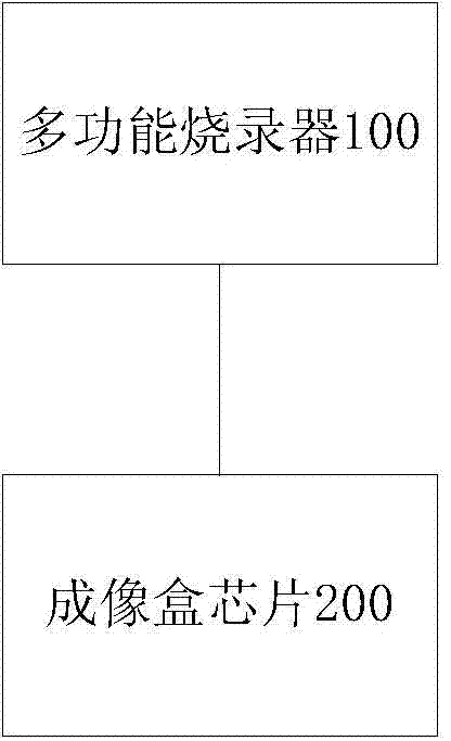
[0049] see figure 1 , an embodiment of an imaging cartridge chip processing device proposed by the present invention, which includes a multi-function programmer 100 and an imaging cartridge chip 200 .

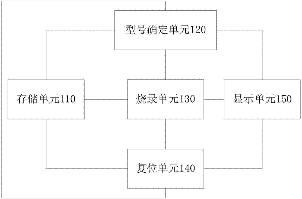
[0050] Wherein, the multi-function programmer 100 is used for storing each group of program information and each group of data information, and determining the model of the imaging cartridge chip 200; 200 burning a corresponding set of program information and / or a set of data information.

[0051] Each set of program information includes each set of complete communication protocols corresponding to the imaging cartridge chip 200 communicating with different types of imaging devices; each set of data information includes each set of chip data information corresponding to different type...


PUM


Abstract

The invention relates to an imaging box chip processing device. The imaging box chip processing device comprises a multifunctional writer and an imaging box chip; the multifunctional writer is used for storing various groups of program information and various groups of data information, and determining the model number of the imaging box chip, or further used for writing a corresponding group of program information and/or a corresponding group of data information to the imaging box chip according to the determined model number; the various groups of program information include various groups of complete communication protocols corresponding to the communication of the imaging box chip with imaging devices of different types; the various groups of data information include various groups of chip data information corresponding to the imaging box chips of different types; the imaging box chip is used for recording the program information and/or the chip data information written by the multifunctional writer to the imaging box chip. The imaging box chip processing device is suitable for processing schemes such as imaging box chip model number determination, writing and resetting; the processing process is convenient. The imaging box chip processing device is accurate and helpful for enhancing the experience of a user and reducing the extra economic losses and cost burden of the user due to time waste.

Description

technical field [0001] The invention relates to the field of electronic technology, in particular to an imaging box chip, a multi-function burner, an imaging box chip processing device and a method. Background technique [0002] The demand for imaging equipment such as printers and copiers continues to increase, and the demand for matching imaging boxes such as toner cartridges in imaging equipment also increases. The imaging box generally includes a chip, and the chip is used for communicating with the imaging device and storing the communication protocol and chip data information between the imaging device and the imaging device. The data includes, for example, the model of the imaging box, the imaging color of the imaging box, the service life of the imaging box, the communication protocol used between the imaging box and a specified type of imaging device or the same type of imaging device in a specified region, etc. Imaging cartridges generally have four imaging colors...

Claims


Application Information

Patent Timeline
IPC IPC(8): G06F9/445
Inventor 毛宏程罗彬段维虎
Owner GUANGZHOU ZHONO ELECTRONICS TECH CO LTD
Why Eureka
Try Eureka