Touch display panel and touch display device

A touch display panel and display area technology, which is applied in the fields of instruments, computing, electrical and digital data processing, etc., can solve the problems of increasing the frame and reducing the competitiveness, and achieve the effect of reducing the size of the frame

CN104571696AActive Publication Date: 2015-04-29WUHAN TIANMA MICRO ELECTRONICS CO LTD +1
3 Cites 11 Cited by

Patent Information

Authority / Receiving Office
CN · China
Current Assignee / Owner
Publication Date
2015-04-29

Smart Images

  • Figure 1
    Figure 1
  • Figure 2
    Figure 2
  • Figure 3
    Figure 3
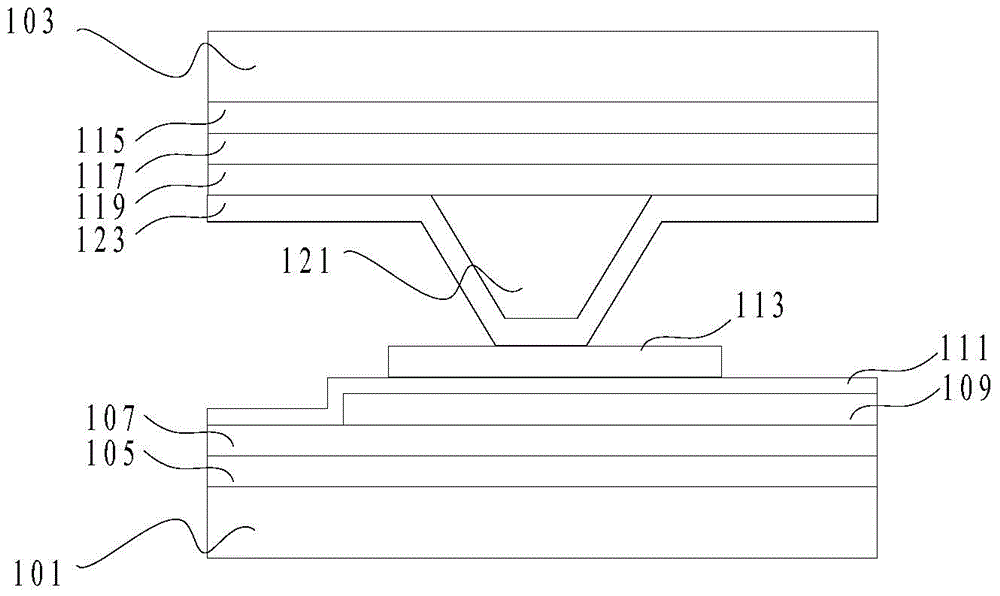
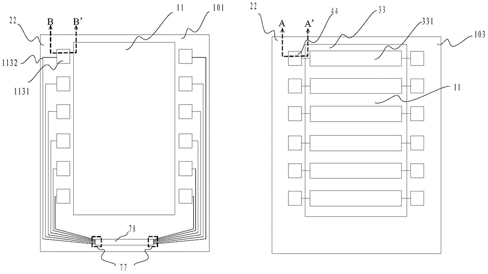
Patent Text Reader

Abstract

The invention discloses a touch control display panel which comprises a first substrate and a second substrate, wherein the first substrate and the second substrate are oppositely arranged and comprise display areas and non-display areas, and the non-display areas surround the display areas; in the display area of the second substrate, one side, which faces towards the first substrate, of the second substrate is provided with a touch layer; in the non-display area of the second substrate, one side, which faces towards the first substrate, of the second substrate is provided with at least one conduction gasket; the conduction gasket is electrically connected with the touch layer; in the non-display area of the first substrate, one side, which faces towards the second substrate, of the first substrate is provided with an organic light-emitting element layer, and the organic light-emitting element layer is provided with a first insulation layer; the first insulation layer is provided with a first conducting layer; the first conducting layer comprises at least one connection gasket and a connecting wire, and the connecting wire is electrically connected with the connection gasket; the projection of the connection gasket on the second substrate is at least partially overlapped with the conduction gasket, and the connection gasket is electrically connected with the conduction gasket.
Need to check novelty before this filing date? Find Prior Art

Description

technical field

[0001] The present invention relates to touch display technology, in particular to an embedded touch display technology. Background technique

[0002] Currently, the integrated active matrix organic light emitting diode display with built-in touch screen is more and more popular due to its ultra-thin screen body.

[0003] Because the touch screen is in the box, both sides can be thinned, which can be thinned to 0.3mm+0.3mm; if the process is thinned after the box is formed, the limit thickness of thinning can even be 0.15mm +0.15mm, very promising. However, the difficulty in making a touch screen is that: on the one hand, the circuits and driving signals of active matrix organic light emitting diode displays are more complex than those of liquid crystal displays, and the pixels of active matrix organic light emitting diode displays are usually pixels containing 6 to 7 thin film transistors circuit, so it is difficult to make a touch screen on the array subs...

Examples

Embodiment Construction

[0016] The following will clearly and completely describe the technical solutions in the embodiments of the present invention with reference to the accompanying drawings in the embodiments of the present invention. Obviously, the described embodiments are only some, not all, embodiments of the present invention. Based on the embodiments of the present invention, all other embodiments obtained by persons of ordinary skill in the art without creative efforts fall within the protection scope of the present invention.

[0017] figure 1 Shown is a cross-sectional view of a touch display panel provided in an embodiment of the present invention in a non-display area, figure 2 The top view of the first substrate and the second substrate of the touch display panel provided by the embodiment of the present invention, next, will combine figure 1 with figure 2 The structure of the touch display panel according to the embodiment of the present invention will be described. First, the t...