Three-dimensional chip testing method and three-dimensional chip testing device

A technology of three-dimensional chips and testing devices, which is applied in the computer field and can solve problems such as low server efficiency

Inactive Publication Date: 2015-05-06
INSPUR BEIJING ELECTRONICS INFORMATION IND
View PDF1 Cites 0 Cited by
  • Summary
  • Abstract
  • Description
  • Claims
  • Application Information

AI Technical Summary

Problems solved by technology

[0005] The invention provides a three-dimensional chip testing method and device, which

Method used


Image

  • Three-dimensional chip testing method and three-dimensional chip testing device
  • Three-dimensional chip testing method and three-dimensional chip testing device

Examples


Embodiment Construction

[0031] In order to make the purpose, technical solutions and advantages of the embodiments of the present invention clearer, the technical solutions in the embodiments of the present invention will be clearly and completely described below in conjunction with the drawings in the embodiments of the present invention. Obviously, the described embodiments It is a part of embodiments of the present invention, but not all embodiments. Based on the embodiments of the present invention, all other embodiments obtained by persons of ordinary skill in the art without making creative efforts belong to the protection scope of the present invention.

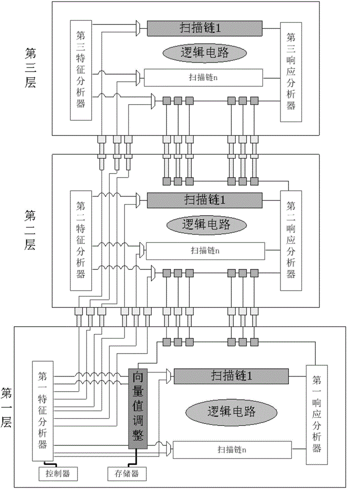
[0032] figure 1 It is a structural schematic diagram of an embodiment of the three-dimensional chip testing device of the present invention, such as figure 1 As shown, the three-dimensional chip testing device includes: a first characteristic analyzer, a second characteristic analyzer, and a third characteristic analyzer; The first layer of...


PUM


Abstract

The invention provides a three-dimensional chip testing method and a three-dimensional chip testing device. The three-dimensional chip testing device comprises a first feature analyzer, a second feature analyzer and a third feature analyzer, wherein the first feature analyzer arranged on a first-layer chip is connected with the first-layer chip, a second-layer chip and a third-layer chip and is used for testing a three-dimensional chip to obtain a first testing result; the second feature analyzer arranged on the second-layer chip is used for testing the second-layer chip to obtain a second testing result; the third feature analyzer arranged on the third-layer chip is used for testing the third-layer chip to obtain a third testing result. The three-dimensional chip is a chip formed by binding of the first-layer chip, the second-layer chip and the third-layer chip. The three-dimensional chip testing method and the three-dimensional chip testing device have the advantages that testing of each chip before binding and the three-dimensional chip obtained after binding of the chips is achieved; the feature analyzers for chip testing are arranged inside the three-dimensional chip, so that the chips can be detected in real time, storage of a great number of data is unneeded, storage capacity is reduced and testing overheads are lowered.

Description

technical field [0001] The invention relates to the field of computers, in particular to a three-dimensional chip testing method and device. Background technique [0002] With the continuous improvement of on-chip integration, three-dimensional chips that bind different chips into a single packaged chip are being widely used. [0003] Usually, the design of a three-dimensional chip requires that the complete circuit module be divided into several parts, which are integrated into different chips, and then the different chips are bound to obtain a complete circuit module. Among them, the test for the three-dimensional chip includes two stages, the first stage is to test each chip before bonding, and the second stage is to test the complete circuit after bonding. [0004] However, the testing device for the three-dimensional chip is arranged outside the chip and needs to store the data of the above two stages, resulting in a very large amount of storage and increasing testing ...

Claims


Application Information

Patent Timeline
IPC IPC(8): G01R31/28
Inventor 屈斌
Owner INSPUR BEIJING ELECTRONICS INFORMATION IND
Why Eureka
Try Eureka