Array substrate

A technology for array substrates and substrate substrates, which is applied in the fields of instruments, computing, and electrical digital data processing, etc., can solve the problem of small pixel aperture ratio, and achieve the effect of increasing the pixel aperture ratio and reducing the size of the black matrix

Active Publication Date: 2016-06-01
SHANGHAI TIANMA MICRO ELECTRONICS CO LTD +1
View PDF3 Cites 11 Cited by
  • Summary
  • Abstract
  • Description
  • Claims
  • Application Information

AI Technical Summary

Problems solved by technology

[0008] An embodiment of the present invention provides an array substrate to solve the problem of a small pixel aperture ratio in the prior art

Method used


Image

  • Array substrate
  • Array substrate
  • Array substrate

Examples


Embodiment Construction

[0048] In order to make the purpose, technical solutions and advantages of the present invention clearer, the technical solutions of the present invention will be clearly and completely described through implementation with reference to the accompanying drawings in the embodiments of the present invention. Obviously, the described embodiments are the embodiment of the present invention. Some, but not all, embodiments. Based on the embodiments of the present invention, all other embodiments obtained by persons of ordinary skill in the art without making creative efforts belong to the protection scope of the present invention.

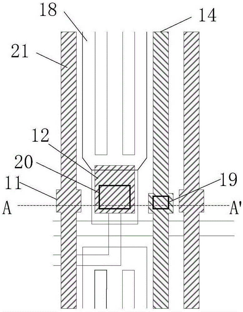
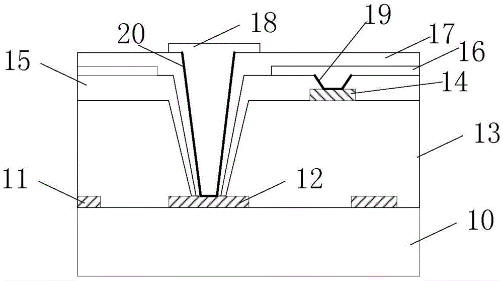
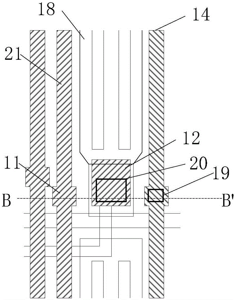
[0049] In order to solve the problems of the existing technology, such as Figure 2A As shown, one embodiment of the present invention provides an array substrate, Figure 2B for Figure 2A Along the cross-sectional view of CC', this embodiment is applicable to the case of increasing the aperture ratio of the pixel.

[0050] Such as Figure 2A and ...


PUM


Abstract

The embodiment of the invention discloses an array substrate. The array substrate comprises a base substrate, a first insulating layer, a plurality of touch control traces, a plurality of touch control electrode blocks, a pixel connecting part and a plurality of pixel electrodes, wherein the first insulating layer is located above the base substrate, at least one first via hole is formed in the first insulating layer, and the at least one first via hole penetrates through the first insulating layer; the touch control traces are located at the bottom part of the at least one first via hole; the touch control electrode blocks are located above the first insulating layer; at least one touch control trace is corresponding to one touch control electrode block, and the touch control electrode block is electrically connected with the at least one corresponding touch control trace; the pixel connecting part is located at the bottom part of the at least one first via hole, and the pixel connecting part is insulated from the touch control traces; the pixel electrodes are located above the first insulating layer, and the pixel electrodes are electrically connected with the pixel connecting part. According to the array substrate disclosed by the invention, the touch control traces and the pixel connecting part share the at least one first via hole; compared with the prior art, the array substrate disclosed by the invention has the advantages that the first via hole number is small, and an aperture size is relatively small, so that a region that liquid crystal molecular orientation is disordered due to the at least one first via hole is reduced, the size of a corresponding black matrix is reduced, and pixel aperture ratio is further increased.

Description

technical field [0001] Embodiments of the present invention relate to display technologies, and in particular to an array substrate. Background technique [0002] With the transformation of display panels to thinner and lighter weight, the integrated design of touch components and LCD panels has become the main development direction of current display panels. The integration of touch components and LCD panels includes "In-cell" and "On-cell" ". The display panel includes an array substrate and a color filter substrate, and the touch components in the In-cell display panel are integrated in the array substrate or the color filter substrate. [0003] Such as Figure 1A Shown is a schematic diagram of an array substrate of an In-cell display panel provided in the prior art, Figure 1B for Figure 1A Sectional view along A-A'. Such as Figure 1A and Figure 1B As shown, the array substrate includes: a substrate 10, a source electrode 11 and a drain electrode 12 located on th...

Claims


Application Information

Patent Timeline
Patent Type & Authority Applications(China)
IPC IPC(8): G06F3/041G02F1/1333
CPCG02F1/13338G06F3/0412G06F3/0443G06F3/04164G06F2203/04103
Inventor 周星耀姚绮君
Owner SHANGHAI TIANMA MICRO ELECTRONICS CO LTD
Why Eureka
Try Eureka