Display substrate and display device

A technology for displaying substrates and display areas, which is applied in the directions of identification devices, optics, instruments, etc., can solve problems such as easy short circuits, and achieve the effects of reducing installation density, reducing the risk of short circuits, and increasing distances

Pending Publication Date: 2017-08-11
BOE TECH GRP CO LTD +1
View PDF6 Cites 29 Cited by
  • Summary
  • Abstract
  • Description
  • Claims
  • Application Information

AI Technical Summary

Problems solved by technology

[0003] The purpose of the embodiments of the present invention is to provide a display substrate and a display device, which are used to solve the problem that the data signal fan-out lines of the respective layers of the gate layer and the source-drain layer of the fan-out area are easily short-circuited between dense lines.

Method used


Image

  • Display substrate and display device
  • Display substrate and display device
  • Display substrate and display device

Examples


Embodiment Construction

[0030] In order to facilitate the understanding of the solution of the present invention, the basic ideas of the solution of the present invention are firstly introduced below:

[0031] In order to reduce the setting density of data signal fan-out lines in the source-drain layer and the gate layer, the inventor considers setting a part of the data signal fan-out lines in other conductive layers. The traces arranged on the touch electrode layer in the fan-out area of ​​the touch screen are relatively sparse, and some traces can be arranged in the touch electrode layer to conduct data signals. The solution provided by the present invention will be described in more detail below with reference to the drawings and embodiments.

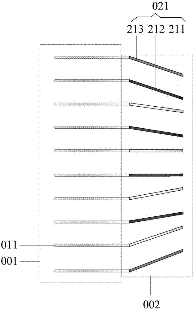
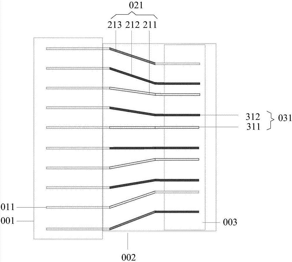
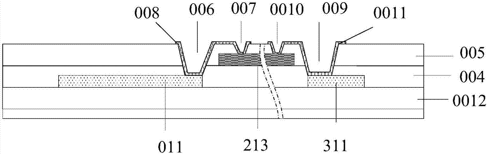
[0032] An embodiment of the present invention provides a display substrate, such as figure 1 As shown, it includes a display area 001 and a fan-out area 002; wherein: the display area 001 includes a plurality of data signal lines 011 located in the source...


PUM


Abstract

The embodiment of the invention discloses a display substrate and a display device. According to the technical scheme, data signal fan-out lines are arranged on a touch electrode layer, a grid layer and a source drain electrode layer, compared with the prior art that data signal fan-out lines are arranged on the grid layer and the source drain electrode layer, the number of the arranged data signal fan-out lines on the grid layer and the source drain electrode layer can be reduced, and thus the setting density of the data signal fan-out lines of the grid layer and/or the source drain electrode layer can be lowered; when a data signal is led out of a display area, the distance between the lines which are aslant arranged is increased, and a short-circuited risk between respective data signal fan-out lines of the grid layer and/or the source drain electrode layer is lowered.

Description

technical field [0001] The present invention relates to the field of display technology, in particular to a display substrate and a display device. Background technique [0002] At present, for high-resolution in-cell (High Definition Full In Cell, HD FIC) touch screens, it is necessary to set up a fan-out (Fanout) area to lead out the signal lines of the display area through wiring. Smaller, but the number of signal lines that need to be drawn out is large. When the data signal lines in the display area are drawn out, the wiring needs to be routed obliquely. , in one structure, there are a total of 2160 data signal lines in the display area. In the current scheme, in the fan-out area, there are 1080 data signal fan-out lines in the gate layer and data signal fan-out lines in the source and drain layers respectively. , to conduct data signals. In this scheme, the data signal fan-out traces of the gate layer in the fan-out area and the data signal fan-out traces of the sourc...

Claims


Application Information

Patent Timeline
Patent Type & Authority Applications(China)
IPC IPC(8): G02F1/1345G02F1/1362G09F9/00G06F3/041
CPCG02F1/1345G02F1/136286G06F3/0412G09F9/00G02F1/13629G06F3/04164H01L27/124G02F1/13338G02F1/1368H01L27/1244
Inventor 尚建兴
Owner BOE TECH GRP CO LTD
Why Eureka
Try Eureka