Chip cleaning container on semiconductor grinding board and its use method

A chip cleaning and grinding plate technology, which is applied in semiconductor/solid-state device manufacturing, electrical components, circuits, etc., can solve the problems that cannot be cleaned and processed on the chip interface on the grinding plate, so as to improve batch production efficiency and prevent scratching and collapse Injury, the effect of protecting the interface

Active Publication Date: 2021-04-06
Shandong Huaguang Optoelectronics Co. Ltd.
View PDF10 Cites 0 Cited by
  • Summary
  • Abstract
  • Description
  • Claims
  • Application Information

AI Technical Summary

Problems solved by technology

[0006] In the above-mentioned patent documents, the chip devices involved are only suitable for the cleaning of individual single-chip or multi-chip chips, and cannot perform the interface cleaning process of chips on the grinding board.

Method used


Image

  • Chip cleaning container on semiconductor grinding board and its use method
  • Chip cleaning container on semiconductor grinding board and its use method
  • Chip cleaning container on semiconductor grinding board and its use method

Examples


Embodiment 1

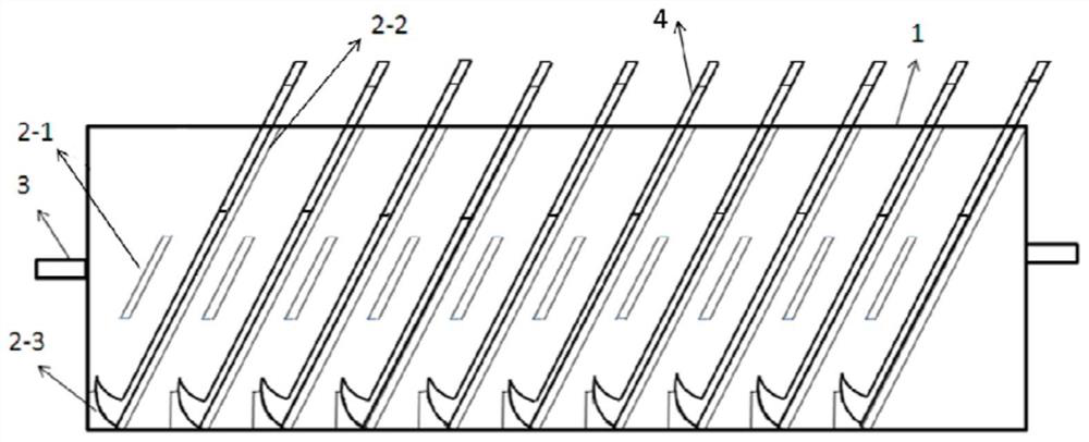
[0049] A chip cleaning container on a semiconductor grinding board, including a container body, the container body is a rectangular cavity with an open top, and ten slot units are arranged inside the container body, and a carrier platform is arranged in the slot unit, such as figure 1 shown.

[0050] The card slot unit includes a card slot front stop, a card slot back stop, and a card slot bottom stop. The number of the card slot front stop and the card slot back stop in a card slot unit is two, and the card slot front stops are arranged symmetrically on the container body. On the inner wall of the container, the back stop of the card slot is symmetrically arranged on the opposite inner wall where the front stop of the card slot is located, and the bottom stop of the card slot is arranged at the bottom of the container body. Both the front block of the card slot and the rear block of the card slot are strip-shaped rectangular blocks.

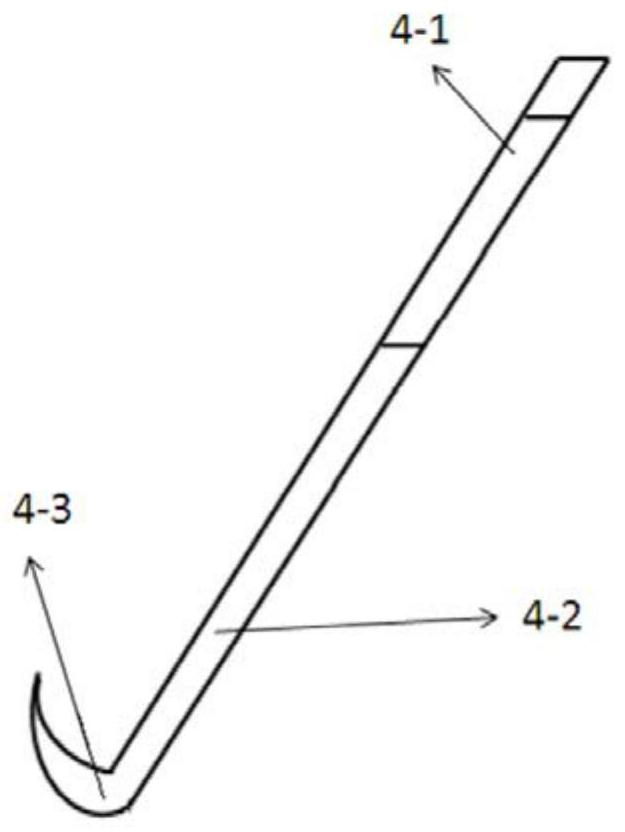
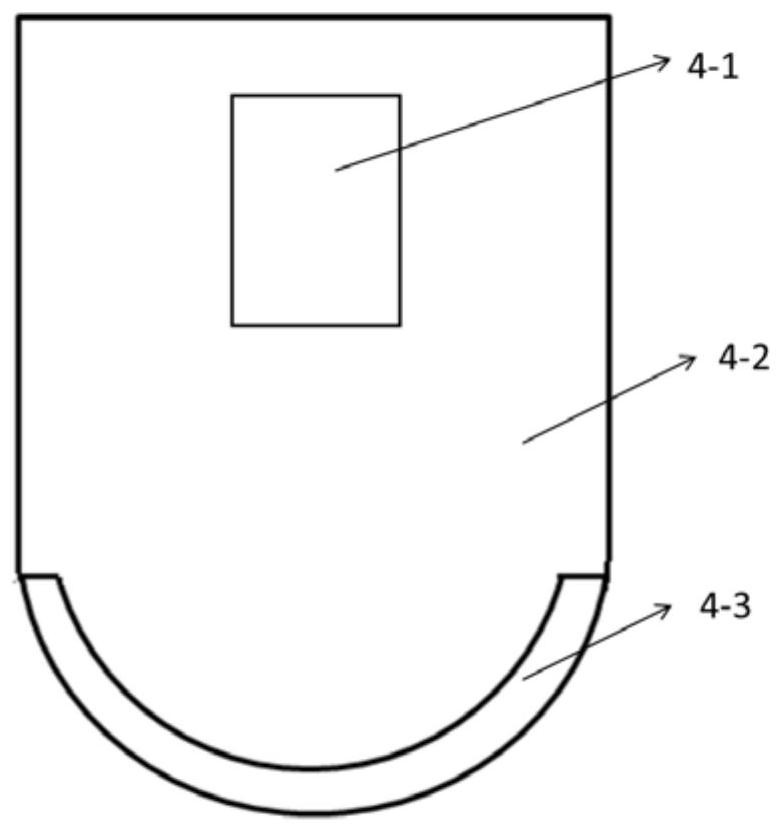
[0051] The carrier table includes the ca...

Embodiment 2

[0054] A chip cleaning container on a semiconductor grinding board, the structure of which is as described in Embodiment 1, the difference is that a container handle is provided at opposite ends of the container body. The handle of the container is arranged on the outside of the side wall of the short side of the rectangle of the container body, and the front stopper and the back stop of the card slot are arranged on the inside of the side wall of the long side of the rectangle of the container body.

Embodiment 3

[0056] A chip cleaning container on a semiconductor grinding board, the structure of which is as described in Embodiment 1, the difference is that the length of the stopper at the front stop of the card slot is shorter than the length of the stopper at the back stop of the card slot.


PUM


Abstract

The invention relates to a chip cleaning container on a semiconductor grinding board and a method for using the same, which belongs to the technical field of semiconductor chip interface cleaning treatment. The device includes a container body with a handle, a slot unit and a movable carrier platform. There is a card slot unit that is symmetrical and repeats at a certain period. The carrier platform is designed in the card slot unit. The grinding plate with the chip is placed on the carrier table. The side moves down along the space of the slot unit on the inner wall of the container body, the outer end of the carrier platform is pushed against the bottom of the slot unit, and the carrier platform together with the grinding plate is submerged into the cavity of the container body. The invention not only provides a grinding plate and a chip interface cleaning / etching process container on the board, but also provides a loading device for the grinding plate, which improves the production efficiency and ensures the cleaning and corrosion treatment of the interface.

Description

technical field [0001] The invention relates to a chip cleaning container on a semiconductor grinding board and a method for using the same, belonging to the technical field of semiconductor chip interface cleaning treatment. Background technique [0002] With the continuous development of semiconductor technology, the requirements for process technology are getting higher and higher, especially for the surface quality of semiconductor chips. In the semiconductor production process, interface cleaning is required in almost every process. The quality of chip cleaning has a serious impact on device performance, and its process quality will directly affect the yield, optoelectronic performance and reliability of the device. At present, the more common cleaning technologies include: wet chemical cleaning, ultrasonic cleaning, megasonic cleaning, scrubbing, high-pressure jet valve, plasma cleaning, RCA cleaning, etc., among which wet chemical cleaning is particularly common. [...

Claims


Application Information

Patent Timeline
Patent Type & Authority Patents(China)
IPC IPC(8): H01L21/67H01L21/673
CPCH01L21/67017H01L21/673
Inventor 刘青苏建汤庆敏肖成峰郑兆河徐现刚
Owner Shandong Huaguang Optoelectronics Co. Ltd.
Why Eureka
Try Eureka