Method of merging blocks in a semiconductor memory device, and semiconductor memory device to perform a method of merging blocks

a semiconductor memory and block technology, applied in the direction of memory adressing/allocation/relocation, instruments, computing, etc., can solve the problem of nand flash memory devices that may drastically decrease in performance, and achieve the effect of improving the overall performance of the semiconductor memory devi

Active Publication Date: 2011-12-01
SAMSUNG ELECTRONICS CO LTD
View PDF2 Cites 29 Cited by
  • Summary
  • Abstract
  • Description
  • Claims
  • Application Information

AI Technical Summary

Benefits of technology

[0008]Some example embodiments provide a method of merging blocks in a semiconductor me

Problems solved by technology

However, overall performance of the NAND flash memory device may drastical

Method used


Image

  • Method of merging blocks in a semiconductor memory device, and semiconductor memory device to perform a method of merging blocks
  • Method of merging blocks in a semiconductor memory device, and semiconductor memory device to perform a method of merging blocks
  • Method of merging blocks in a semiconductor memory device, and semiconductor memory device to perform a method of merging blocks

Examples


Embodiment Construction

[0064]Reference will now be made in detail to the embodiments of the present general inventive concept, examples of which are illustrated in the accompanying drawings, wherein like reference numerals refer to the like elements throughout. The embodiments are described below in order to explain the present general inventive concept while referring to the figures. The present general inventive concept may, however, be embodied in many different forms and should not be construed as limited to the example embodiments set forth herein. In the drawings, the sizes and relative sizes of layers and regions may be exaggerated for clarity.

[0065]It will be understood that when an element or layer is referred to as being “on,”“connected to” or “coupled to” another element or layer, it can be directly on, connected or coupled to the other element or indirectly on, connected or coupled to the other element (e.g., layer or intervening elements or layers may be present). In contrast, when an element...


PUM


Abstract

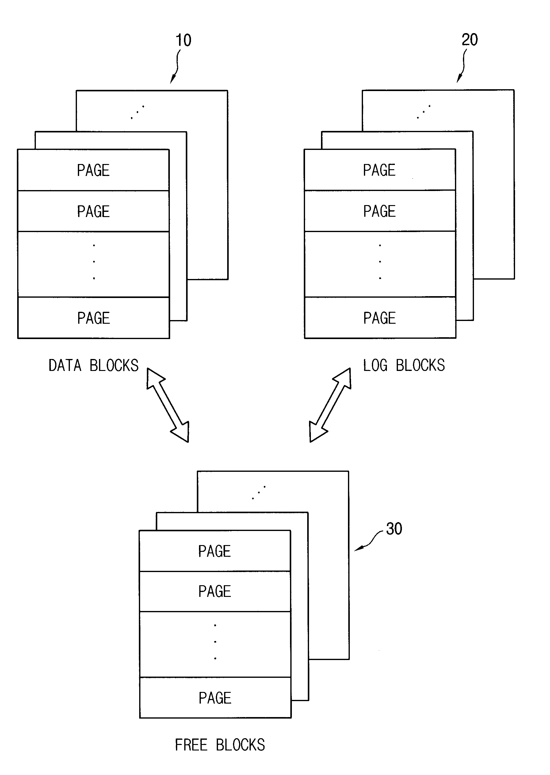
In a method of merging blocks in a semiconductor memory device according to example embodiments, a plurality of data are written into one or more first blocks using a first program method. One or more merge target blocks that are required to be merged are selected among the one or more first blocks. A merge-performing block for a block merge operation is selected among the one or more first blocks and one or more second blocks. A plurality of merge target data are written from the merge target blocks into the merge-performing block using a second program method that is different from the first program method.

Description

CROSS-REFERENCE TO RELATED APPLICATIONS[0001]This application claims priority under 35 U.S.C. §119 from Korean Patent Application No. 2010-0048367, filed on May 25, 2010, in the Korean Intellectual Property Office (KIPO), the entire content of which is incorporated herein by reference in its entirety.BACKGROUND OF THE INVENTION[0002]1. Field of the Invention[0003]Example embodiments according to the present general inventive concepts relate to semiconductor memory devices. More particularly, the example embodiments relate to methods of merging blocks in semiconductor memory devices, and semiconductor memory devices that perform methods of merging blocks.[0004]2. Description of the Related Art[0005]Semiconductor memory devices can be roughly divided into volatile memory devices and nonvolatile memory devices according to whether they retain stored data when disconnected from power. Recently, as electronic devices require lower power consumption and smaller size, a NAND flash memory d...

Claims


Application Information

Patent Timeline
IPC IPC(8): G06F12/02G06F12/00
CPCG06F12/0246G06F2212/7205G06F2212/7202
InventorKIM, MIN-SEOKPARK, KI-TAE
OwnerSAMSUNG ELECTRONICS CO LTD