Supercharge Your Innovation With Domain-Expert AI Agents!

Display device and manufacturing method thereof

a technology of display device and manufacturing method, which is applied in the direction of semiconductor devices, instruments, electrical devices, etc., can solve the problem of short circuit between adjacent signal lines

Active Publication Date: 2016-09-22
SAMSUNG DISPLAY CO LTD
View PDF2 Cites 1 Cited by
  • Summary
  • Abstract
  • Description
  • Claims
  • Application Information

AI Technical Summary

Benefits of technology

The patent text describes a display device that prevents wiring shorts caused by silver (Ag) that can occur between adjacent signal lines. This is achieved by using an insulating layer that has silver (Ag) removed from its edge, which prevents the formation of such wiring shorts. The technical effect of this invention is to improve the reliability and efficiency of the display device by preventing wiring shorts and reducing the likelihood of malfunctions.

Problems solved by technology

However, silver (Ag) ions may remain after the silver (Ag) is deposited and then spread in a boundary portion of an insulating layer disposed near the signal line, thereby causing a wiring short between adjacent signal lines.

Method used


Image

  • Display device and manufacturing method thereof
  • Display device and manufacturing method thereof
  • Display device and manufacturing method thereof

Examples


Embodiment Construction

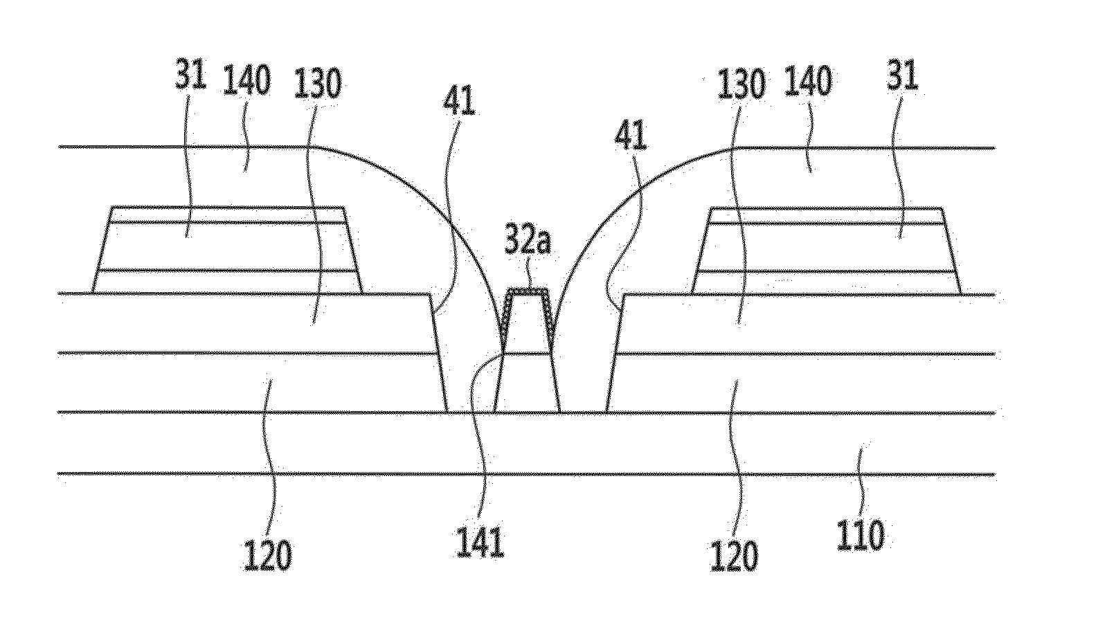
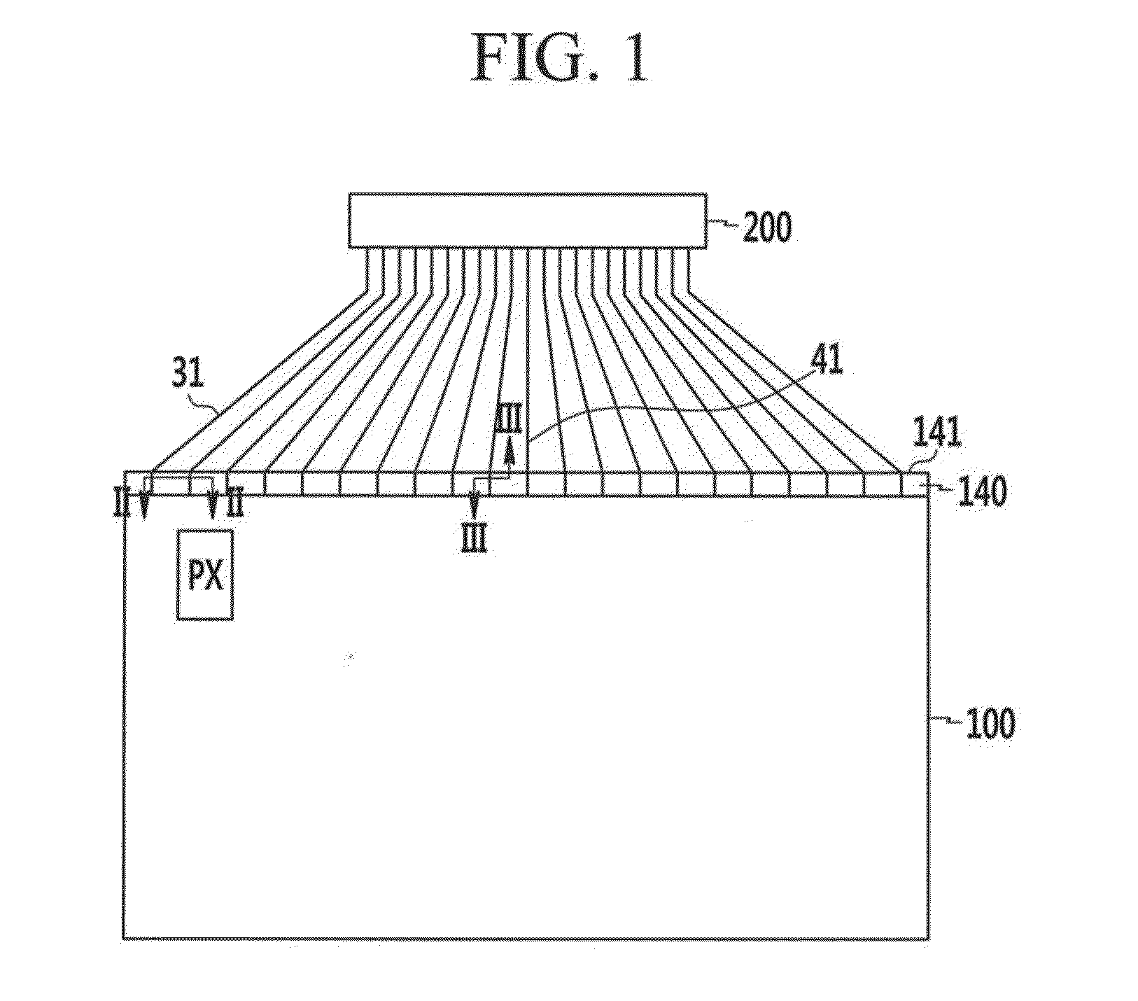
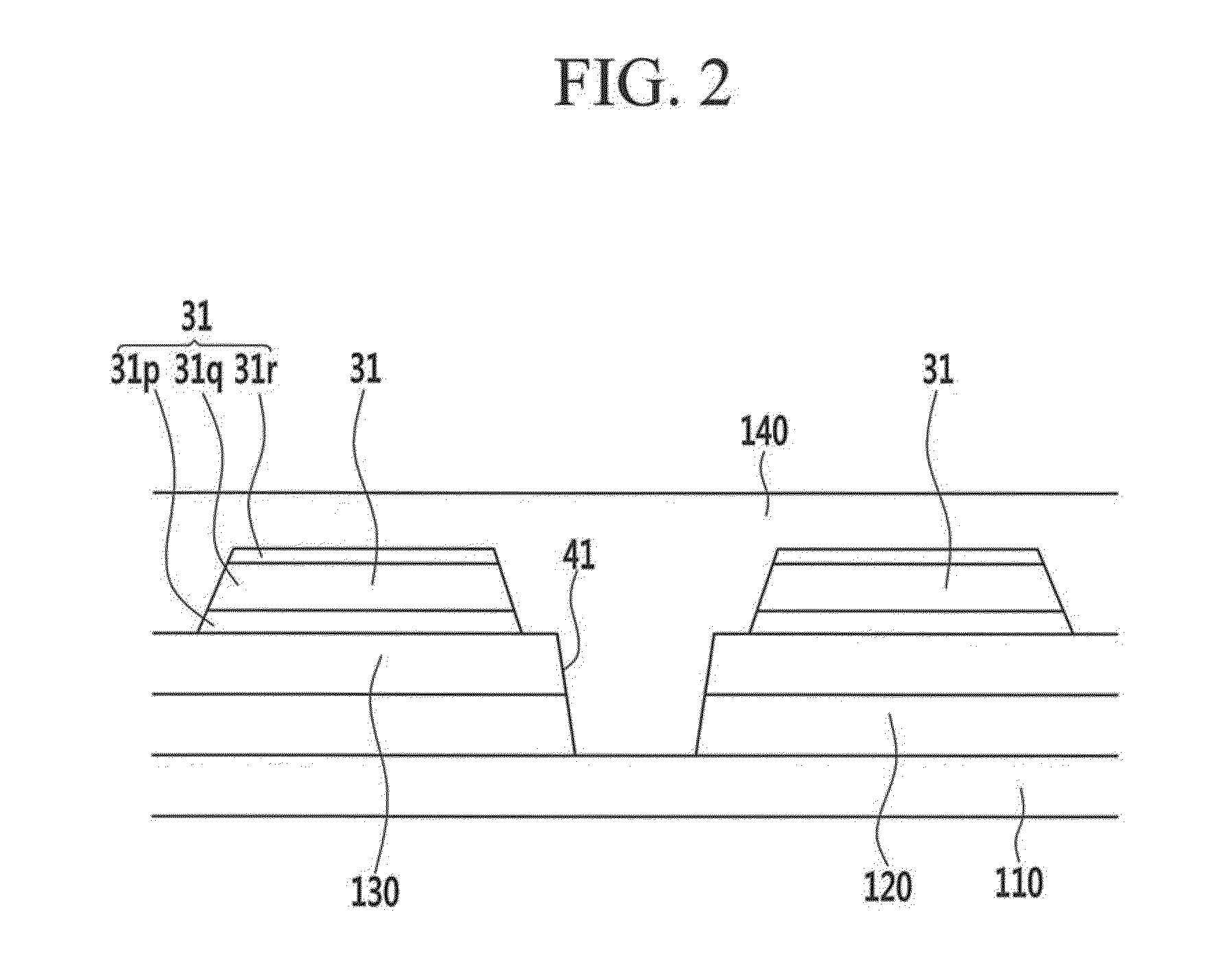
[0029]Aspects and features of some exemplary embodiments of the present invention are described more fully herein with reference to the accompanying drawings, in which some exemplary embodiments of the present invention are shown. The present invention may, however, be embodied in different forms and should not be construed as limited to the embodiments set forth herein. Rather, these embodiments are provided in order to convey the scope of the present invention to those skilled in the art. As those skilled in the art would realize, the described embodiments may be modified in various different ways, all without departing from the spirit or scope of the present invention.

[0030]In the drawings, the thickness of layers, films, panels, regions, etc., may be exaggerated for clarity. Like reference numerals designate like elements throughout the specification. It will be understood that when an element such as a layer, film, region, or substrate is referred to as being “on” another eleme...


PUM


Abstract

A display device includes: a first substrate comprising a display area including a plurality of pixels, and a peripheral area around the display area; a plurality of driving signal transmission lines on the first substrate and arranged in the peripheral area; a first insulating layer on the first substrate and arranged under the plurality of driving signal transmission lines; and a second insulating layer on a portion of the plurality of driving signal transmission lines and arranged in the display area, and the first insulating layer includes a trench between two driving signal transmission lines adjacent to each other among the plurality of driving signal transmission lines, and an edge portion of the second insulating layer overlaps the trench.

Description

CROSS-REFERENCE TO RELATED APPLICATION[0001]This application claims priority to and the benefit of Korean Patent Application No. 10-2015-0036961, filed on Mar. 17, 2015 in the Korean Intellectual Property Office, the entire content of which is incorporated herein by reference.BACKGROUND[0002]1. Field[0003]Aspects of embodiments of the present invention relate to a display device and a manufacturing method of the display device.[0004]2. Description of the Related Art[0005]As an area of a display device is increased, a signal line is elongated, and accordingly resistance of the signal line is increased. As described above, if the resistance of the signal line is increased, a signal delay or a voltage drop may be generated, and to solve these problems, it is necessary to form the signal line using a material having low, resistivity. Accordingly, silver (Ag) as one among the materials having low resistivity may be used to form a wire such as a data line.[0006]However, silver (Ag) ions m...

Claims


Application Information

Patent Timeline
IPC IPC(8): H01L27/12
CPCH01L27/1262H01L27/1244H01L27/1259G02F1/13452G02F1/13458
Inventor KIM, DEUK JONGKIM, HYO JINPARK, WON MO
Owner SAMSUNG DISPLAY CO LTD
Features
  • R&D
  • Intellectual Property
  • Life Sciences
  • Materials
  • Tech Scout
  • Unparalleled Data Quality
  • Higher Quality Content
  • 60% Fewer Hallucinations
Learn More