
Liquid crystal display device having OCB mode liquid crystal layer and method of fabricating the same
a liquid crystal layer and liquid crystal display technology, applied in non-linear optics, instruments, optics, etc., can solve the problems of high power consumption, pixel bend-transiting may still occur, and require a lot of time, so as to achieve sufficient bend-transiting without degrading display quality
- Summary
- Abstract
- Description
- Claims
- Application Information
AI Technical Summary
Benefits of technology
Problems solved by technology
Method used
Image

Examples
Embodiment Construction
[0021]In the following detailed description, exemplary embodiments of the present invention are shown and described, by way of illustration. As those skilled in the art would recognize, the described exemplary embodiments may be modified in various ways, all without departing from the spirit or scope of the present invention. Accordingly, the drawings and description are to be regarded as illustrative in nature, rather than restrictive. There may be parts shown in the drawings, or parts not shown in the drawings, that are not discussed in the specification, as they are not essential to a complete understanding of the invention. Like reference numerals designate like elements. In a case where it is stated that one layer is formed “on” another layer, this may refer to the one layer being directly on the another layer or to a third layer being interposed between the one layer and the another layer.
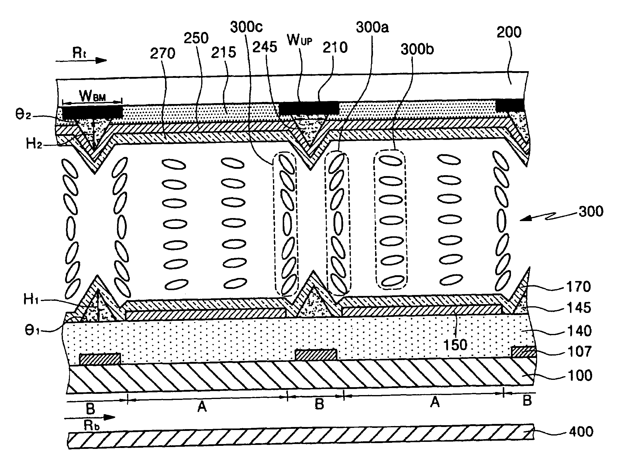
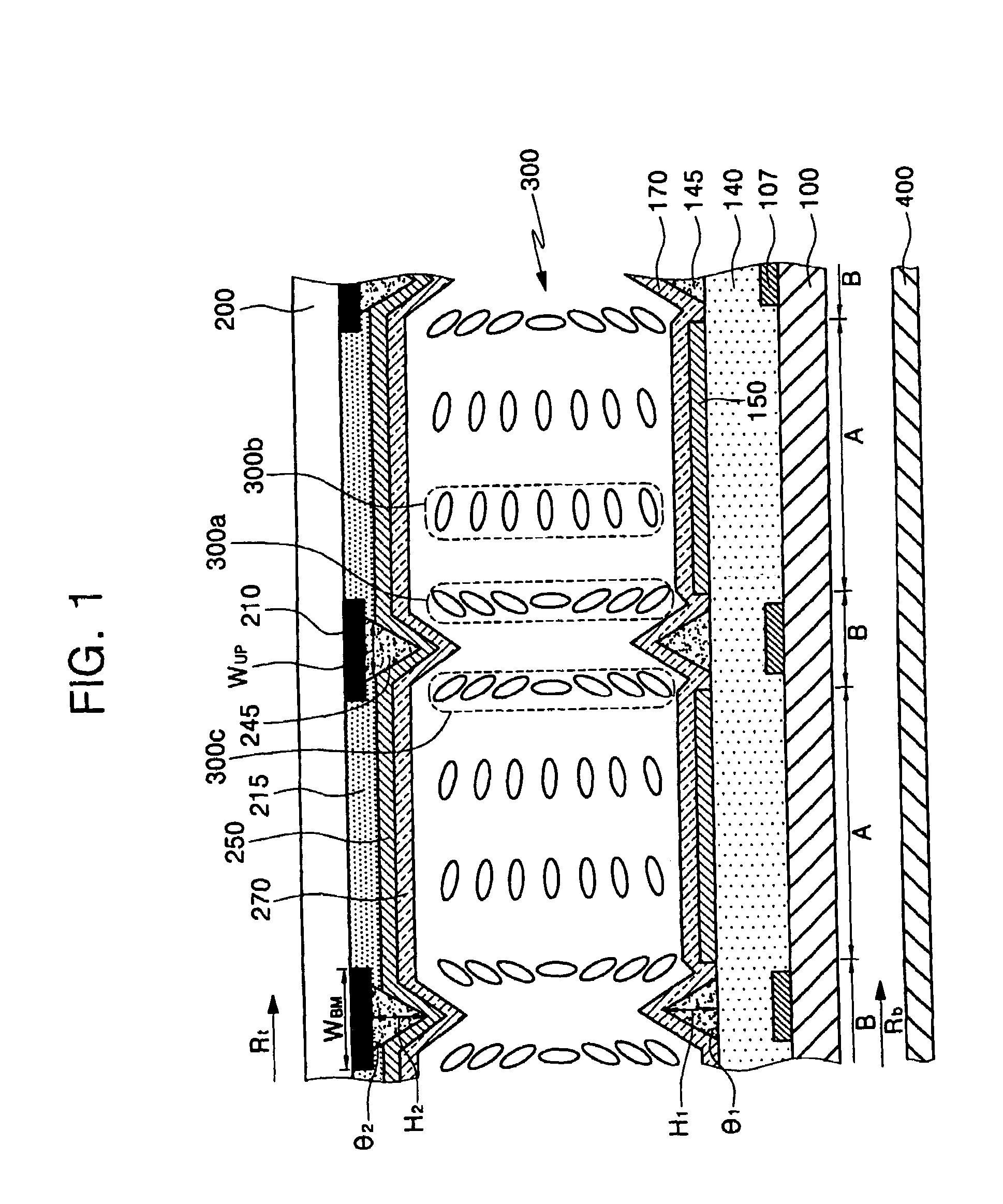
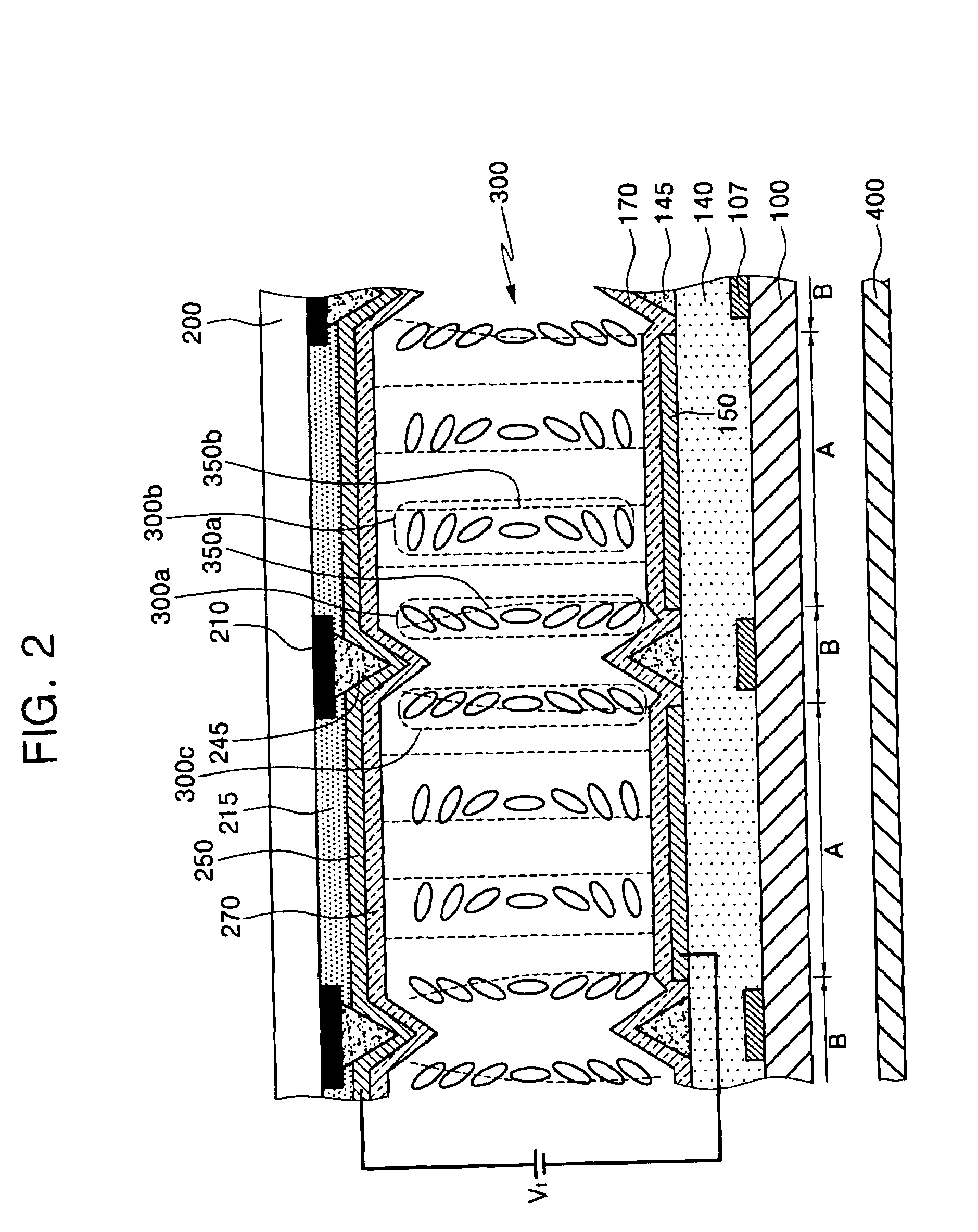
[0022]FIG. 1 is a cross-sectional view illustrating an LCD device according to an embodim...
PUM
| Property | Measurement | Unit |
|---|---|---|
| angle | aaaaa | aaaaa |
| angle | aaaaa | aaaaa |
| angle | aaaaa | aaaaa |
Abstract
Description
Claims
Application Information